LTC1040CN 查看數據表(PDF) - Linear Technology
零件编号
产品描述 (功能)
生产厂家
LTC1040CN Datasheet PDF : 12 Pages
| |||
LTC1040
ABSOLUTE AXI U RATI GS
(Note 1)
Total Supply Voltage (V+ to V –) ............................... 18V
lnput Voltage ........................ (V+ + 0.3V) to (V – – 0.3V)
Operating Temperature Range
LTC1040C ..................................... – 40°C ≤ TA ≤ 85°C
LTC1040M (OBSOLETE) .................... – 55°C to 125°C
Storage Temperature Range ................. – 55°C to 150°C
Lead Temperature (Soldering, 10 sec).................. 300°C
Output Short-Circuit Duration .......................Continuous
UW U
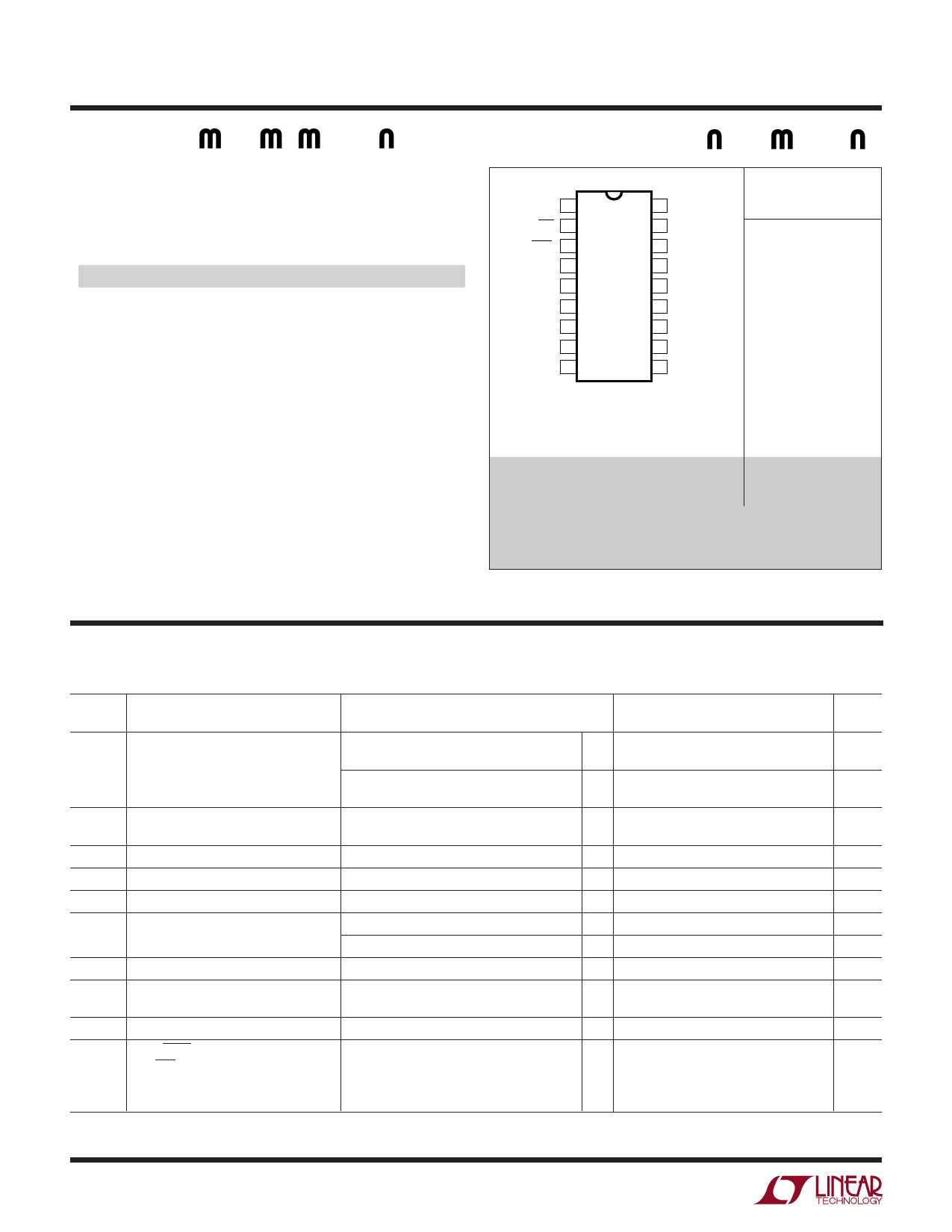
PACKAGE/ORDER I FOR ATIO
STROBE 1
ON/OFF 2
A+B 3
AOUT 4
A1+ 5
A1– 6
A2+ 7
A2– 8
GND 9
TOP VIEW
18 V+
17 VP-P
16 OSC
15 BOUT
14 B1+
13 B1–
12 B2+
11 B2–
10 V–
N PACKAGE
SW PACKAGE
18-LEAD PDIP 18-LEAD PLASTIC SO WIDE
TJMAX = 110°C, θJA = 120°C/W (N)
TJMAX = 125°C, θJA = 85°C/W (SW)
ORDER PART
NUMBER
LTC1040CN
LTC1040CSW
J PACKAGE
18-LEAD CERDIP
TJMAX = 150°C, θJA = 80°C/W
LTC1040MJ
LTC1040CJ
OBSOLETE PACKAGE
Consider the N18 Package as an Alternate Source
Consult LTC Marketing for parts specified with wider operating temperature ranges.
ELECTRICAL CHARACTERISTICS The q denotes the specifications which apply over the full operating
temperature range, otherwise specifications are at TA = 25°C. Test conditions: V+ = 5V, V – = – 5V, unless otherwise noted.
SYMBOL PARAMETER
CONDITIONS
LTC1040M/LTC1040C
MIN
TYP
MAX
UNITS
VOS
Offset Voltage (Note 2)
Split Supplies ±2.8V to ±6V
q
Single Supply (V– = GND) 2.8V to 6V
Split Supplies ±6V to ±8V
q
Single Supply (V– = GND) 6V to 15V
±0.3
± 0.75
mV
±1
±4.5
mV
Tracking Error Between
Input Pairs (Notes 2 and 3)
Split Supplies ±2.8V to ±8V
q
Single Supplies (V– = GND) 2.8 to 16V
0.05
0.1
%
IBIAS
RIN
CMR
PSR
IS(ON)
IS(OFF)
tD
VOH
VOL
Input Bias Current
Average Input Resistance
Common Mode Range
Power Supply Range
Power Supply ON Current (Note 5)
Power Supply OFF Current (Note 5)
Response Time (Note 6)
A, B, A + B and
ON/OFF Outputs (Note 7)
Logic “1” Output Voltage
Logic “0” Output Voltage
OSC = GND
fS = 1kHz (Note 4)
Split Supplies
Single Supplies (V– = GND)
V+ = 5V, VP-P On
V+ = 5V, VP-P Off
LTC1040C
LTC1040M
V+ = 4.75V, lOUT = – 360µA
V+ = 4.75V, lOUT = 1.6mA
±0.3
nA
q
20
30
MΩ
q
V–
V+
V
q ±2.8
±8
V
q
2.8
16
V
q
1.2
3
mA
q
0.001
0.5
µA
q
0.001
5
µA
60
80
100
µs
q
2.4
4.4
V
q
0.25
0.4
V
1040fa
2
Share Link: 