LTC1153C 查看數據表(PDF) - Linear Technology
零件编号
产品描述 (功能)
生产厂家
LTC1153C Datasheet PDF : 16 Pages
| |||
LTC1153
PI FU CTIO S
Drain Sense Pin
The drain sense pin is compared against the supply pin
voltage. If the voltage at this pin is more than 100mV
below the supply pin, the input latch will trip and the
MOSFET switch will be turned off.
This pin is also a high impedance CMOS gate with ESD
protection and therefore should not be forced beyond the
power supply rails.
Some loads, such as large supply capacitor, lamps, or
motors require high inrush currents. An RC time is added
between the sense resistor and the drain sense pin to
ensure that the drain sense circuitry does not false trigger
during start-up. This trip delay can be set from a few
microseconds to many seconds. However, very long de-
lays may put the MOSFET switch in risk of being destroyed
by a short-circuit condition. (see Applications Information
Section).
Status Pin
The status pin is an open-drain output which is driven low
whenever the breaker is tripped. A 51k pull-up resistor
should be connected between this output and a logic
supply. The status pins of multiple LTC1153s can be OR’d
together if independent fault sensing is not required. No
connection is required to this pin when not in use.
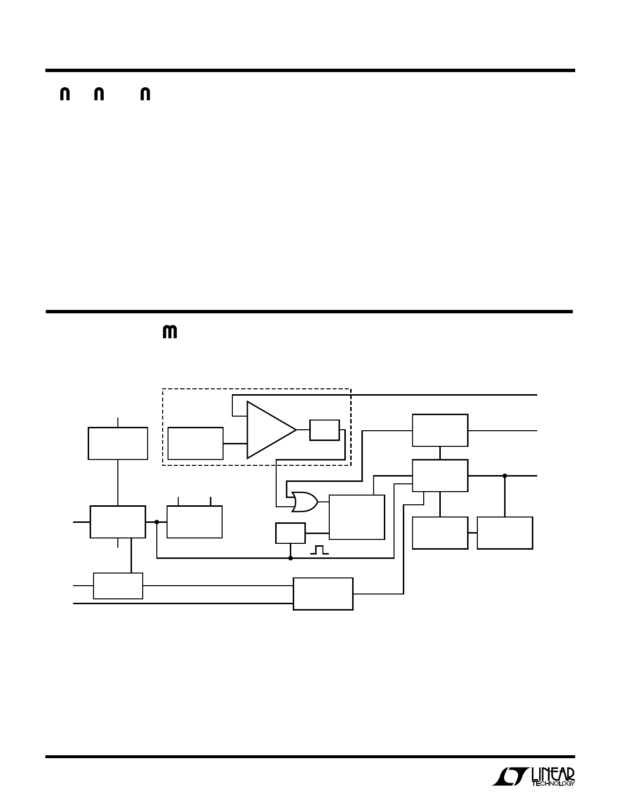
BLOCK DIAGRA
VS
LOW STANDBY
CURRENT
REGULATOR
ANALOG SECTION
100mV
REFERENCE
COMP
10µs
DELAY
INPUT
TIMER
CAP
STATUS
TTL-TO-CMOS
CONVERTER
GND
AUTO-RESET
TIMER
ANALOG DIGITAL
VOLTAGE
REGULATORS
ONE
SHOT
R
INPUT
LATCH
S
FAULT DETECTION
AND STATUS
OUTPUT DRIVER
SHUTDOWN
TTL-TO-CMOS
CONVERTER
GATE CHARGE
AND DISCHARGE
CONTROL LOGIC
DRAIN
SENSE
SHUTDOWN
GATE
OSCILLATOR
AND CHARGE
PUMP
FAST/SLOW
GATE CHARGE
LOGIC
LTC1153 • BD01
6
Share Link: 