LTC1155I 查看數據表(PDF) - Linear Technology
零件编号
产品描述 (功能)
生产厂家
LTC1155I Datasheet PDF : 16 Pages
| |||
LTC1155
U
OPERATIO
Gate Charge Pump
Gate drive for the power MOSFET is produced by an
adaptive charge pump circuit that generates a gate voltage
substantially higher than the power supply voltage. The
charge pump capacitors are included on-chip and, there-
fore, no external components are required to generate the
gate drive.
Drain Current Sense
The LTC1155 is configured to sense the drain current of
the power MOSFET in high side applications. An internal
100mV reference is compared to the drop across a sense
resistor (typically 0.002Ω to 0.1Ω) in series with the drain
lead. If the drop across this resistor exceeds the internal
100mV threshold, the input latch is reset and the gate is
quickly discharged by a large N-channel transistor.
Controlled Gate Rise and Fall Times
When the input is switched ON and OFF, the gate is
charged by the internal charge pump and discharged in a
controlled manner. The charge and discharge rates have
been set to minimize RFI and EMI emissions in normal
operation. If a short circuit or current overload condition
is encountered, the gate is discharged very quickly (typi-
cally a few microseconds) by a large N-channel transistor.
APPLICATI S I FOR ATIO
Protecting the MOSFET
The MOSFET is protected against destruction by removing
drive from the gate as soon as an overcurrent condition is
detected. Resistive and inductive loads can be protected
with no external time delay. Large capacitive or lamp
loads, however, require that the overcurrent shutdown
function be delayed long enough to start the load but short
enough to ensure the safety of the MOSFET.
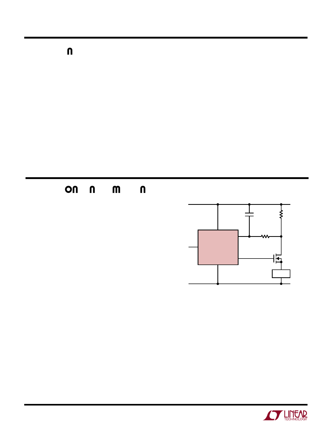
Example Calculations
Consider the circuit of Figure 1. A power MOSFET is driven
by one side of an LTC1155 to switch a high inrush current
load. The drain sense resistor is selected to limit the
maximum DC current to 3.3A.
RSEN = VSEN/ITRIP
= 0.1/3.3A
= 0.03Ω
A time delay is introduced between RSEN and the drain
sense pin of the LTC1155 which provides sufficient delay
to start a high inrush load such as large supply capacitors.
In this example circuit, we have selected the IRLZ34
because of its low RDS(ON )(0.05Ω with VGS = 5V). The FET
VS = 5.0V
VS
DS1
IN1 LTC1155
GND
G1
CDLY
0.22µF
RDLY
270k
RSEN
0.03Ω
IRLZ34
GND
LOAD
1155 F01
Figure 1. Adding an RC Delay
drops 0.1V at 2A and, therefore, dissipates 200mW in
normal operation (no heat sinking required).
If the output is shorted to ground, the current through the
FET rises rapidly and is limited by the RDS(ON) of the FET,
the drain sense resistor and the series resistance be-
tween the power supply and the FET. Series resistance in
the power supply can be substantial and attributed to
many sources including harness wiring, PCB traces,
supply capacitor ESR, transformer resistance or battery
resistance.
6
Share Link: 