LTC1157 查看數據表(PDF) - Linear Technology
零件编号
产品描述 (功能)
生产厂家
LTC1157 Datasheet PDF : 8 Pages
| |||
LTC1157
PI FU CTIO S
Input Pins: The LTC1157 input pins are active high and
activate the charge pump circuitry when switched ON. The
LTC1157 logic inputs are high impedance CMOS gates
with ESD protection diodes to ground and supply and
therefore should not be forced beyond the power supply
rails.
Gate Drive Pins: The gate drive pin is either driven to
ground when the switch is turned OFF or driven above the
supply rail when the switch is turned ON. This pin is a
relatively high impedance when driven above the rail (the
equivalent of a few hundred kΩ). Care should be taken to
minimize any loading of this pin by parasitic resistance to
ground or supply.
Supply Pin: The supply pin of the LTC1157 should never
be forced below ground as this may result in permanent
damage to the device. A 300Ω resistor should be inserted
in series with the ground pin if negative supply voltage
transients are anticipated.
U
OPERATIO
The LTC1157 is a dual micropower MOSFET driver de-
signed specifically for operation at 3.3V and 5V and
includes the following functional blocks:
3.3V Logic Compatible Inputs
The LTC1157 inputs have been designed to accommodate
a wide range of 3.3V and 5V logic families. Approximately
50mV of hysteresis is provided to ensure clean switching.
An ultra low standby current voltage regulator provides
continuous bias for the logic-to-CMOS converter. The
logic-to-CMOS converter output enables the rest of the
circuitry. In this way the power consumption is kept to an
absolute minimum in the standby mode.
Gate Charge Pump
Gate drive for the power MOSFET is produced by an
internal charge pump circuit which generates a gate volt-
age substantially higher than the power supply voltage.
The charge pump capacitors are included on-chip and
therefore no external components are required to generate
the gate drive.
Controlled Gate Rise and Fall Times
When the input is switched ON and OFF, the gate is
charged by the internal charge pump and discharged in a
controlled manner. The charge and discharge rates have
been set to minimize RFI and EMI emissions.
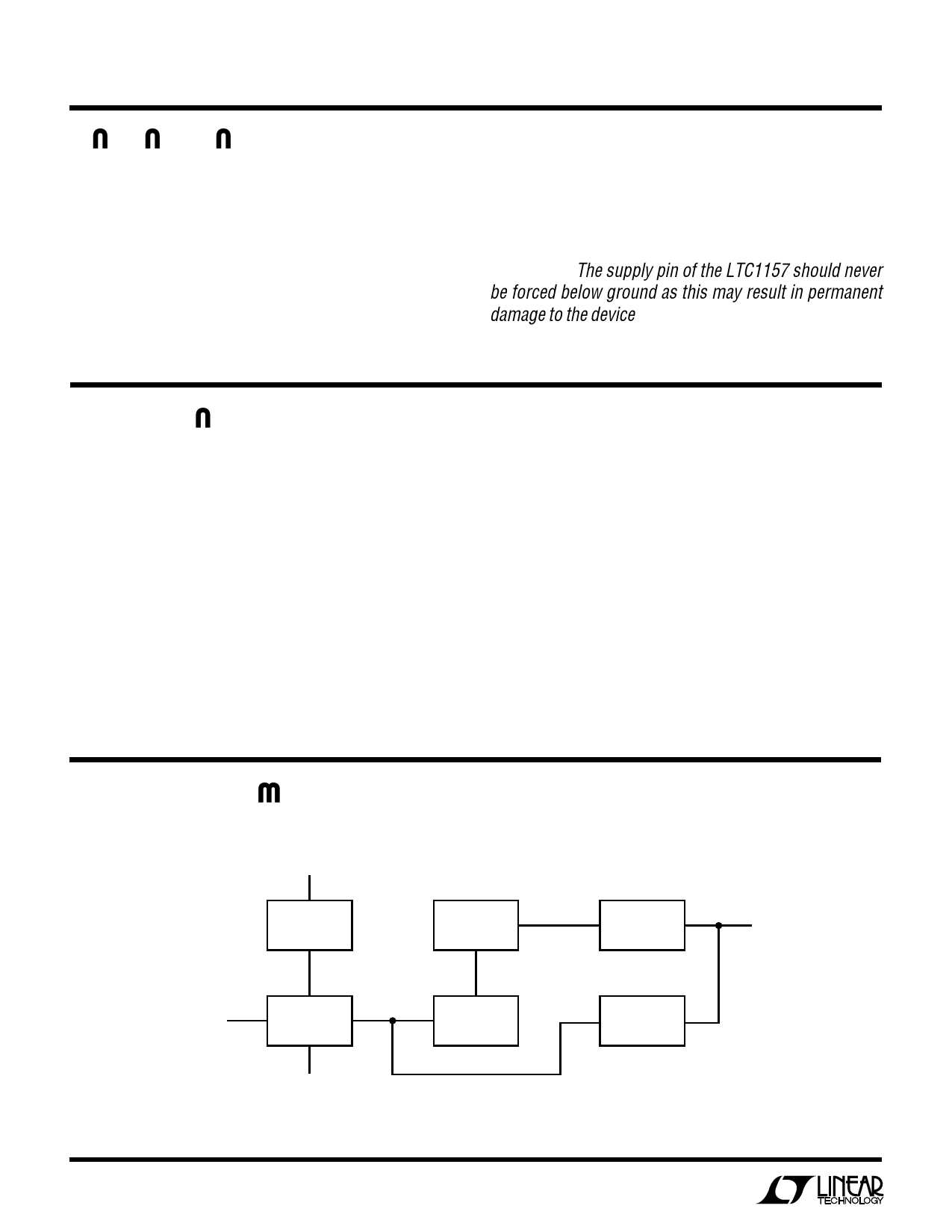
W
BLOCK DIAGRA (One Channel)
VS
LOW STANDBY
CURRENT
REGULATOR
HIGH
FREQUENCY
OSCILLATOR
CHARGE
PUMP
GATE
INPUT
LOGIC-TO-CMOS
CONVERTER
GND
VOLTAGE
REGULATOR
GATE
DISCHARGE
LOGIC
LTC1157 • BD
4
Share Link: 