LTC1157 查看數據表(PDF) - Linear Technology
零件编号
产品描述 (功能)
生产厂家
LTC1157 Datasheet PDF : 8 Pages
| |||
UU W U
APPLICATIO S I FOR ATIO
MOSFET Selection
The LTC1157 is designed to operate with both standard
and logic level N-channel MOSFET switches. The choice of
switch is determined primarily by the operating supply
voltage.
Logic Level MOSFET Switches at 3.3V
Logic level switches should be used with the LTC1157
when powered from 2.7V to 4V. Although there is some
variation among manufacturers, logic level MOSFET
switches are typically rated with VGS = 4V with a maximum
continuous VGS rating of ±10V. RDS(ON) and maximum
VDS ratings are similar to standard MOSFETs and there is
generally little price differential. Logic level MOSFETs are
frequently designated by an “L” and are usually available
in surface mount packaging. Some logic level MOSFETs
are rated up to ±15V and can be used in applications which
require operation over the entire 2.7V to 5.5V range.
Standard MOSFET Switches at 5V
Standard N-channel MOSFET switches should be used
with the LTC1157 when powered from 4V to 5.5V supply
as the built-in charge pump produces ample gate drive to
fully enhance these switches when powered from a 5V
nominal supply. Standard N-channel MOSFET switches
are rated with VGS = 10V and are generally restricted to a
maximum of ±20V.
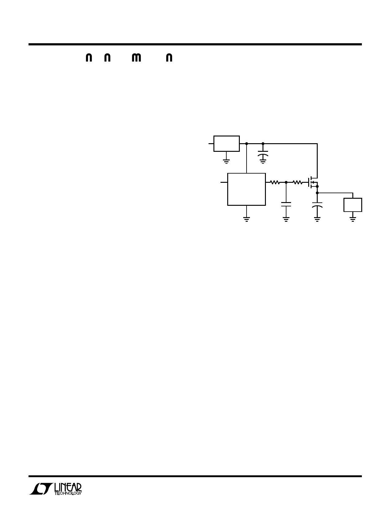
Powering Large Capacitive Loads
Electrical subsystems in portable battery-powered equip-
ment are typically bypassed with large filter capacitors to
reduce supply transients and supply induced glitching. If
not properly powered however, these capacitors may
themselves become the source of supply glitching.
For example, if a 100µF capacitor is powered through a
switch with a slew rate of 0.1V/µs, the current during start-
up is:
ISTART = C(dV/dt)
= (100 × 10 – 6) (1 × 10 5)
= 10A
LTC1157
Obviously, this is too much current for the regulator (or
output capacitor) to supply and the output will glitch by as
much as a few volts.
The start-up current can be substantially reduced by
limiting the slew rate at the gate of an N-channel switch as
shown in Figure 1. The gate drive output of the LTC1157
3.3V
VIN LT1129-3.3
+
3.3µF
ON/0FF
VS
IN1
R1
100k
G1
1/2 LTC1157
GND
R2
1k
MTD3055EL
C1
+
CLOAD
0.1µF
100µF
3.3V
LOAD
LTC1157 • TA02
Figure 1. Powering a Large Capacitive Load
is passed through a simple RC network, R1 and C1, which
substantially slows the slew rate of the MOSFET gate to
approximately 1.5 × 10 –4 V/µs. Since the MOSFET is
operating as a source follower, the slew rate at the source
is essentially the same as that at the gate, reducing the
start-up current to approximately 15mA which is easily
managed by the system regulator. R2 is required to
eliminate the possibility of parasitic MOSFET oscillations
during switch transitions. Also, it is good practice to
isolate the gates of paralleled MOSFETs with 1k resistors
to decrease the possibility of interaction between switches.
Reverse Battery Protection
The LTC1157 can be protected against reverse battery
conditions by connecting a 300Ω resistor in series with
the ground pin. The resistor limits the supply current to
less than 12mA with – 3.6V applied. Since the LTC1157
draws very little current while in normal operation, the
drop across the ground resistor is minimal. The 3.3V µP
(or control logic) can be protected by adding 10k resistors
in series with the input pins.
5
Share Link: 