LTC1159 查看數據表(PDF) - Linear Technology
零件编号
产品描述 (功能)
生产厂家
LTC1159 Datasheet PDF : 20 Pages
| |||
LTC1159
LTC1159-3.3/LTC1159-5
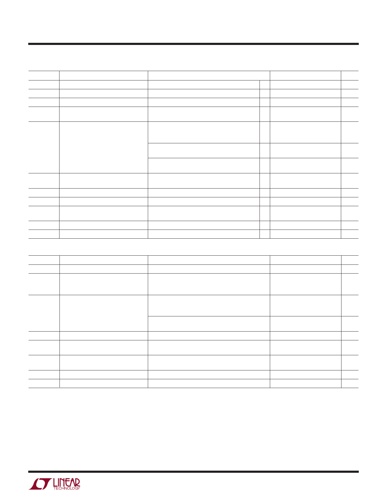
ELECTRICAL CHARACTERISTICS The q denotes specifications which apply over the full operating
temperature range, otherwise specifications are at TA = 25°C. VIN = 12V, VSHDN1 = 0V (Note 3), unless otherwise noted.
SYMBOL
PARAMETER
CONDITIONS
MIN TYP MAX
VCC
VIN – VCC
VEXT – VCC
VP-GATE – VIN
VSENSE+ –
VSENSE –
VSNDN1
Internal Regulator Voltage
VCC Dropout Voltage
EXTVCC Switch Drop
P-Gate to Source Voltage (Off)
Current Sense Threshold Voltage
LTC1159
LTC1159-3.3
LTC1159-5
SHDN1 Threshold
LTC1159CG, LTC1159-3.3, LTC1159-5
VIN = 12V to 40V, EXTVCC = 0V, ICC = 10mA
VIN = 4V, EXTVCC = Open, ICC = 10mA
VIN = 12V, EXTVCC = 5V, ISWITCH = 10mA
VIN = 12V
VIN = 40V
VSENSE– = 5V, VFB = 1.32V (Forced)
VSENSE– = 5V, VFB = 1.15V (Forced)
VSENSE– = 3.4V (Forced)
VSENSE– = 3.1V (Forced)
VSENSE– = 5.2V (Forced)
VSENSE– = 4.7V (Forced)
q 4.25
4.5
4.75
300 400
250 350
– 0.2
0
– 0.2
0
25
q 130
150
170
25
q 130
150
170
25
q 130
150
170
0.5
0.8
2
VSHDN2
ISHDN2
ICT
tOFF
tr, tf
SHDN2 Threshold
Shutdown 2 Input Current
CT Pin Discharge Current
Off-Time (Note 5)
Driver Output Transition Times
VSHDN2 = 5V
VOUT in Regulation
VOUT = 0V
CT = 390pF, ILOAD = 700mA, VIN = 10V
CL = 3000pF (Pins P-Drive and N-Gate), VIN = 6V
0.8
1.4
2
12
20
50
70
90
2
10
4
5
6
100 200
UNITS
V
mV
mV
V
V
mV
mV
mV
mV
mV
mV
V
V
µA
µA
µA
µs
ns
– 40°C ≤ TA ≤ 85°C (Note 6)
SYMBOL
PARAMETER
VFB
Feedback Voltage (LTC1159 Only)
VOUT
Regulated Output Voltage
LTC1159-3.3
LTC1159-5
IIN
VIN Pin Current (Note 4)
Normal
Shutdown
IEXTVCC
VCC
EXTVCC Pin Current (Note 4)
Internal Regulator Voltage
CONDITIONS
VIN = 9V
ILOAD = 700mA
ILOAD = 700mA
VIN = 12V, EXTVCC = 5V
VIN = 40V, EXTVCC = 5V
VIN = 12V, VSHDN2 = 2V
VIN = 40V, VSHDN2 = 2V
EXTVCC = 5V, Sleep Mode
VIN = 12V to 40V, EXTVCC = 0V, ICC = 10mA
MIN TYP MAX UNITS
1.2
1.25
1.3
V
3.17 3.30 3.43
V
4.85 5.05 5.25
V
200
µA
300
µA
15
µA
25
µA
250
µA
4.5
V
VSENSE+ –
VSENSE –
VSHDN2
tOFF
Current Sense Threshold Voltage
SHDN2 Threshold
Off-Time (Note 5)
Low Threshold (Forced)
High Threshold (Forced)
CT = 390pF, ILOAD = 700mA, VIN = 10V
25
mV
125
150
175
mV
0.8
1.4
2
V
3.5
5
6.5
µs
Note 1: Absolute Maximum Ratings are those values beyond which the life
of a device may be impaired.
Note 2: TJ is calculated from the ambient temperature TA and power
dissipation PD according to the following formulas:
LTC1159CG, LTC1159CG-3.3, LTC1159CG-5: TJ = TA + (PD • 135°C/W)
LTC1159CN, LTC1159CN-3.3, LTC1159CN-5: TJ = TA + (PD • 80°C/W)
LTC1159CS, LTC1159CS-3.3, LTC1159CS-5: TJ = TA + (PD • 110°C/W)
Note 3: On LTC1159 versions which have a SHDN1 pin, it must be at
ground potential for testing.
Note 4: The LTC1159 VIN and EXTVCC current measurements exclude
MOSFET driver currents. When VCC power is derived from the output via
EXTVCC, the input current increases by (IGATECHG • Duty Cycle)/(Efficiency).
See Typical Performance Characteristics and Applications Information.
Note 5: In applications where RSENSE is placed at ground potential, the off-
time increases approximately 40%.
3
Share Link: 