LTC1159 查看數據表(PDF) - Linear Technology
零件编号
产品描述 (功能)
生产厂家
LTC1159 Datasheet PDF : 20 Pages
| |||
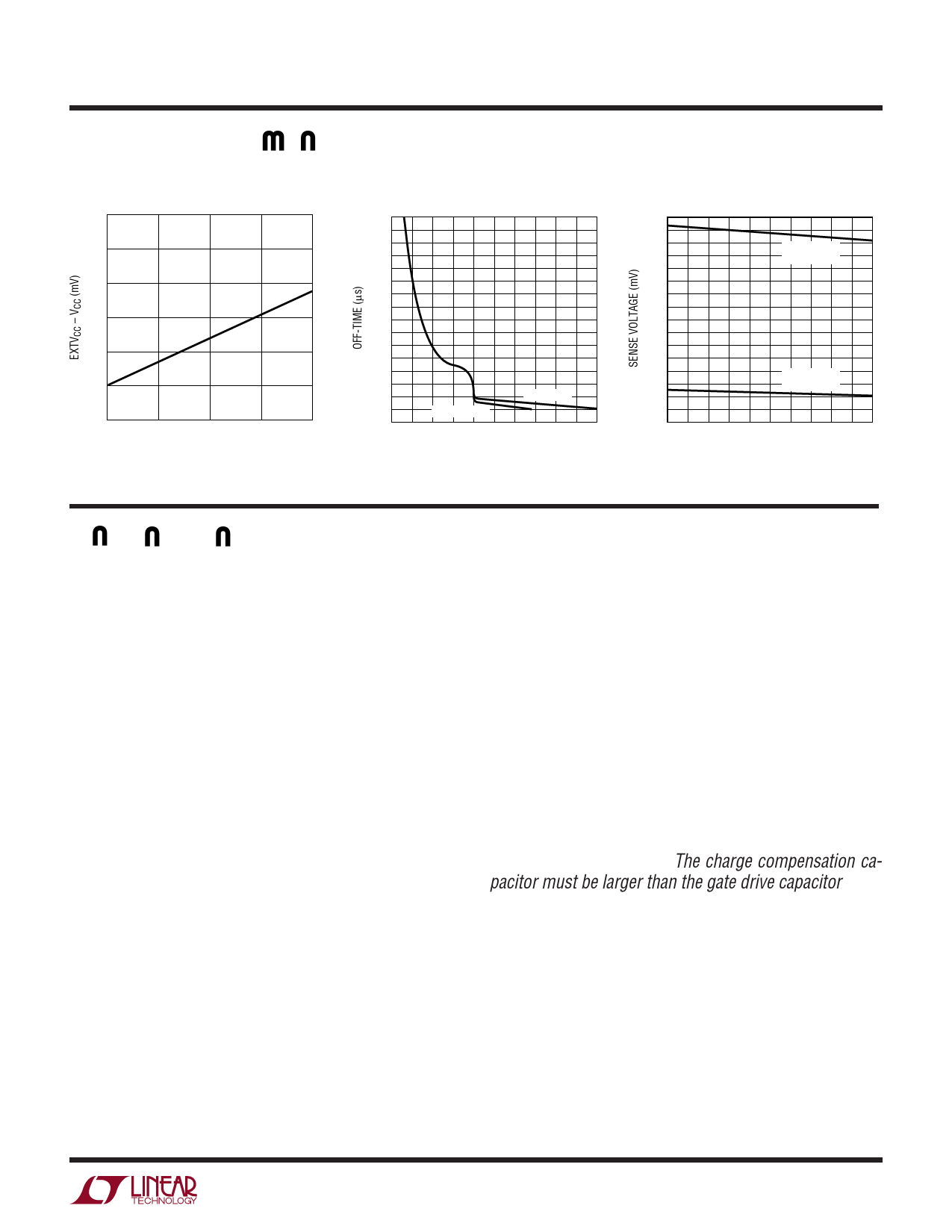
TYPICAL PERFOR A CE CHARACTERISTICS
LTC1159
LTC1159-3.3/LTC1159-5
EXTVCC Switch Drop
600
500
400
300
200
100
0
0
5
10
15
20
SWITCH CURRENT (mA)
LTC1159 • TPC07
Off-Time vs VOUT
80
70
60
50
40
30
20
10
LTC1159-5
LTC1159-3.3
0
0
1
2
3
4
5
OUTPUT VOLTAGE (V)
LTC1159 • TPC08
Current Sense Threshold Voltage
160
140
MAXIMUM
THRESHOLD
120
100
80
60
40
MINIMUM
THRESHOLD
20
0
0
20
40
60
80 100
TEMPERATURE (°C)
LTC1159 • TPC09
PI FU CTIO S
VIN: Main Supply Input Pin.
SGND: Small-Signal Ground. Must be routed separately
from other grounds to the (–) terminal of COUT.
PGND: Driver Power Grounds. Connect to source of N-
channel MOSFET and the (–) terminal of CIN.
VCC: Outputs of internal 4.5V linear regulator, EXTVCC
switch, and supply inputs for driver and control circuits.
The driver and control circuits are powered from the higher
of the 4.5V regulator or EXTVCC voltage. Must be closely
decoupled to power ground.
CT: External capacitor CT from this pin to ground sets the
operating frequency. (The frequency is also dependent on
the ratio VOUT/VIN.)
ITH: Gain Amplifier Decoupling Point. The current com-
parator threshold increases with the ITH pin voltage.
VFB: For the LTC1159 adjustable version, the VFB pin
receives the feedback voltage from an external resistive
divider used to set the output voltage.
SENSE–: Connects to internal resistive divider which sets
the output voltage in fixed output versions. The SENSE– pin
is also the (–) input of the current comparator.
SENSE+: The (+) Input for the Current Comparator. A built-
in offset between the SENSE+ and SENSE– pins, in conjunc-
tion with RSENSE, sets the current trip threshold.
N-Gate: High Current Drive for the Bottom N-Channel
MOSFET. The N-Gate pin swings from ground to VCC.
P-Gate: Level-Shifted Gate Drive Signal for the Top
P-Channel MOSFET. The voltage swing at the P-gate pin is
from VIN to VIN – VCC.
P-Drive: High Current Gate Drive for the Top P-Channel
MOSFET. The P-drive pin(s) swing(s) from VCC to ground.
CAP: Charge Compensation Pin. A capacitor to VCC pro-
vides charge required by the P-gate level-shift capacitor
during supply transitions. The charge compensation ca-
pacitor must be larger than the gate drive capacitor.
SHDN1: This pin shuts down the control circuitry only (VCC
is not affected). Taking SHDN1 pin high turns off the
control circuitry and holds both MOSFETs off. This pin
must be at ground potential for normal operation.
SHDN2: Master Shutdown Pin. Taking SHDN2 high shuts
down VCC and all control circuitry.
5
Share Link: 