LTC1165 查看數據表(PDF) - Linear Technology
零件编号
产品描述 (功能)
生产厂家
LTC1165 Datasheet PDF : 8 Pages
| |||
U
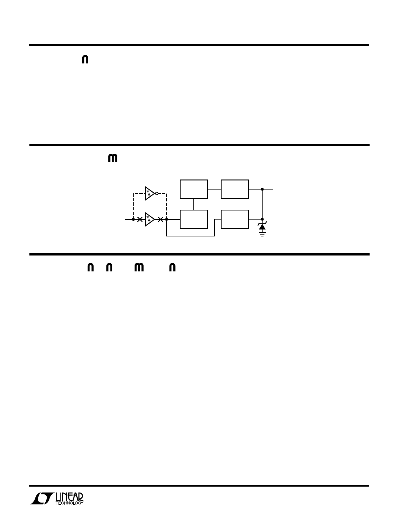
OPERATIO
Gate Charge Pump
Gate drive for the power MOSFET is produced by an
internal charge pump circuit which generates a gate volt-
age substantially higher than the power supply voltage.
The charge pump capacitors are included on chip and
therefore no external components are required to generate
gate drive.
W
BLOCK DIAGRA (One Channel)
LTC1163/LTC1165
Controlled Gate Rise and Fall Times
When the input is switched ON and OFF, the gate is
charged by the internal charge pump and discharged in a
controlled manner. The charge and discharge rates have
been set to minimize RFI and EMI emissions.
INPUT
LTC1165
LTC1163
HIGH
FREQUENCY
OSCILLATOR
BIAS
GENERATOR
CHARGE
PUMP
GATE
DISCHARGE
LOGIC
GATE
14V
LTC1163/65 • BD
UU W U
APPLICATIO S I FOR ATIO
Logic-Level MOSFET Switches
The LTC1163/LTC1165 are designed to operate with
logic-level N-channel MOSFET switches. Although there
is some variation among manufacturers, logic-level
MOSFET switches are typically rated with VGS = 4V with
a maximum continuous VGS rating of ±10V. RDS(ON) and
maximum VDS ratings are similar to standard MOSFETs
and there is generally little price differential. Logic-level
MOSFETs are frequently designated by an “L” and are
usually available in surface mount packaging. Some
logic-level MOSFETs are rated with VGS up to ±15V and
can be used in applications which require operation over
the entire 1.8V to 6V range.
Powering Large Capacitive Loads
Electrical subsystems in portable battery-powered equip-
ment are typically bypassed with large filter capacitors to
reduce supply transients and supply induced glitching. If
not properly powered however, these capacitors may
themselves become the source of supply glitching.
For example, if a 100µF capacitor is powered through a
switch with a slew rate of 0.1V/µs, the current during start-
up is:
ISTART = C(∆V/∆t)
= (100 × 10 – 6)(1 × 10⁵)
= 10A
Obviously, this is too much current for the regulator (or
output capacitor) to supply and the output will glitch by as
much as a few volts.
The startup current can be substantially reduced by limit-
ing the slew rate at the gate of an N-channel as shown in
Figure 1. The gate drive output of the LTC1163/LTC1165
is passed through a simple RC network, R1 and C1, which
substantially slows the slew rate of the MOSFET gate to
approximately 1.5 × 10 – 4V/µs. Since the MOSFET is
operating as a source follower, the slew rate at the source
is essentially the same as that at the gate, reducing the
startup current to approximately 15mA which is easily
5
Share Link: 