LTC1164A 查看數據表(PDF) - Linear Technology
零件编号
产品描述 (功能)
生产厂家
LTC1164A Datasheet PDF : 16 Pages
| |||
LTC1164
PI FU CTIO S
Power Supplies (Pins 7,19)
They should be bypassed with 0.1µF ceramic disc. Low
noise, non-switching, power supplies are recommended.
The device operates with a single 5V supply and with dual
supplies. The absolute maximum operating power supply
voltage is ±8.25V. Supply reversal is not allowed and can
cause latch up. When using dual supplies, loads between
the positive and negative supply (even light loads) can
cause momentary supply reversal during power-up. A
clamp diode from each supply to ground will prevent
reversal and latch problems.
Clock (Pin 18)
For ±5V supplies the logic threshold level is 1.8V. For ±8V
and 0 to 5V supplies the logic threshold level is 2.8V. The
logic threshold levels vary ±100mV over the full military
temperature range. The recommended duty cycle of the
input clock is 50%, although for clock frequencies below
500kHz the clock “on” time can be as low as 200ns. The
maximum clock frequency for single 5V supply and Q
values <5 is 500kHz and for ±5V supplies and above is
1MHz. The clock input can be applied before power is
turned on as long as there is no chance the clock signal will
go below the V– supply.
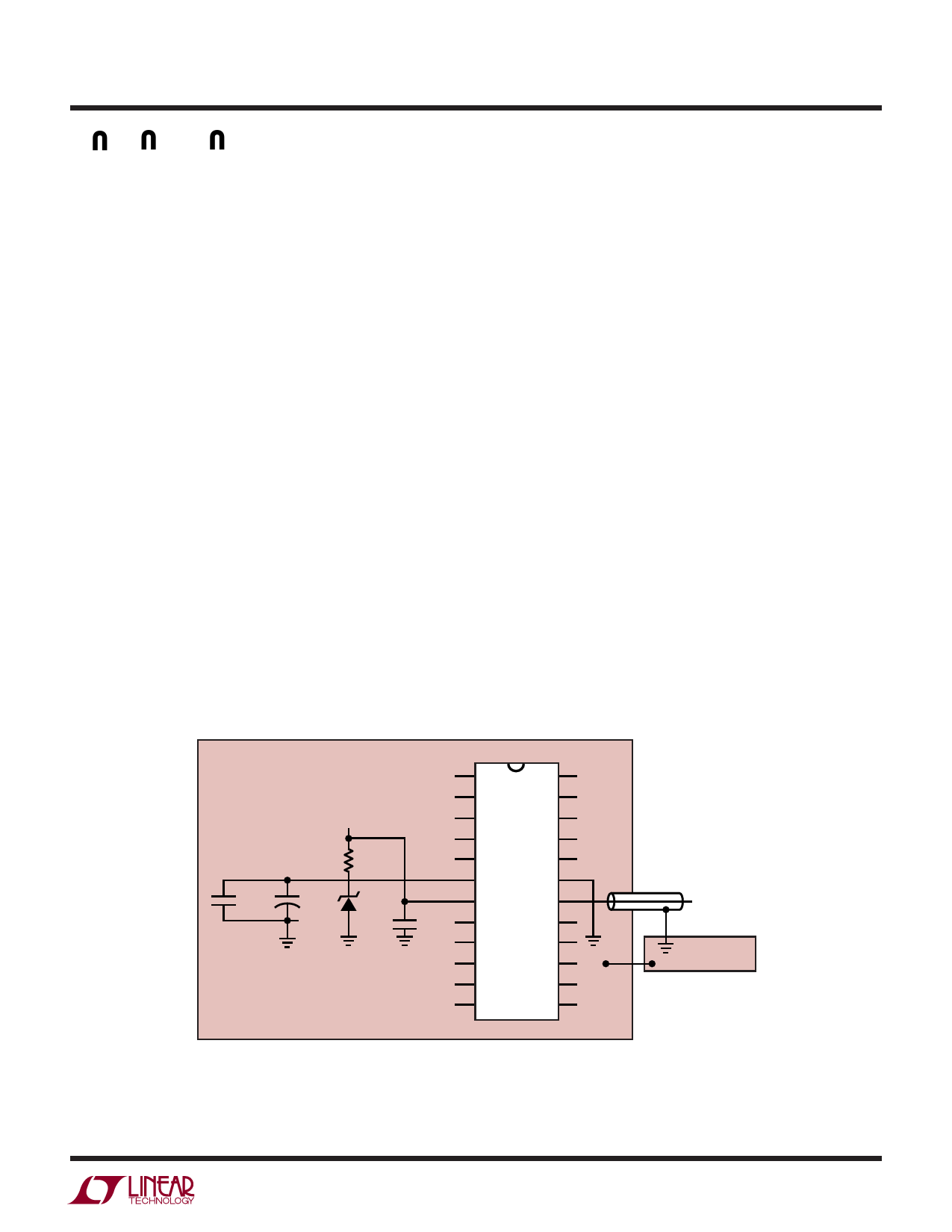
AGND (PIN 6)
When the LTC1164 operates with dual supplies, Pin 6
should be tied to system ground. When the LTC1164
operates with a single positive supply, the analog ground
pin should be tied to 1/2 supply and it should be bypassed
with a 4.7µF solid tantalum in parallel with a 0.1µF ceramic
disc, Figure 2. The positive input of all the internal op
amps, as well as the common reference of all the internal
switches, are internally tied to the analog ground pin.
Because of this, a very “clean” ground is recommended.
50/100 (Pin 17)
By tying Pin 17 to V+, all filter sections operate with a clock-
to-center frequency ratio internally set at 50:1. When Pin
17 is at mid-supplies, sections B and C operate with (fCLK/
fO) = 50:1 and sections A and D operate at (100:1). When
Pin 17 is shorted to the negative supply pin, all filter
sections operate with (fCLK/fO) = 100:1.
+
0.1µF
V+
4.7µF
7.5k
V+/2
LT1004*
0.1µF
ANALOG
GROUND
PLANE
1
24
2
23
3
22
4
LTC1164
21
5
20
6 AGND
7 V+
8
9
V – 19
CLK 18
17
50/100
16
10
15
11
14
12
13
NOTE: PIN 5, 8, 20, IF NOT USED, SHOULD BE CONNECTED TO PIN 6.
*LT1004 CAN BE REPLACED WITH A 7.5k RESISTOR FOR V+ >6.5V
LTC1164 • PD01
Figure 2. Single Supply Operation
CLOCK INPUT
V+ = 15V, TRIP VOLTAGE = 7V
V+ = 10V, TRIP VOLTAGE = 6.4V
V+ = 5V, TRIP VOLTAGE = 3V
TO DIGITAL
GROUND
1164fa
7
Share Link: 