LTC1411 查看數據表(PDF) - Linear Technology
零件编号
产品描述 (功能)
生产厂家
LTC1411 Datasheet PDF : 16 Pages
| |||
LTC1411
TEST CIRCUITS
Load Circuits for Access Timing
DN
1k
CL
5V
1k
DN
CL
(A) Hi-Z TO VOH AND VOL TO VOH
(B) Hi-Z TO VOL AND VOH TO VOL
1411 TC01
Load Circuits for Output Float Delay
DN
1k
CL
5V
1k
DN
CL
(A) VOH TO Hi-Z
(B) VOL TO Hi-Z
1411 TC02
APPLICATIO S I FOR ATIO
CONVERSION DETAILS
The LTC1411 uses a successive approximation algorithm
and an internal sample-and-hold circuit to convert an
analog signal to a 14-bit parallel output. The ADC is
complete with a precision reference, internal clock and a
programmable input range. The device is easy to interface
with microprocessors and DSPs. (Please refer to the
Digital Interface section for the data format.)
Conversions are started by a falling edge on the CONVST
input. Once a conversion cycle has begun, it cannot be
restarted. Between conversions, the ADC acquires the
analog input in preparation for the next conversion. In the
acquire phase, a minimum time of 100ns will provide
enough time for the sample-and-hold capacitors to ac-
quire the analog signal.
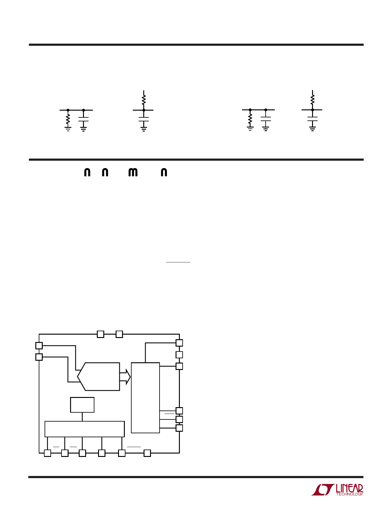
1 AIN+
2 AIN–
10
30
AVP DVP
+
14-BIT
– ADC
INTERNAL
CLOCK
14
OUTPUT
DRIVERS
CONTROL LOGIC
OVDD
29
OGND 28
D13
12
•
•
•
D0 25
BUSY
27
OTR
26
SLP NAP PGA0 PGA1 CONVST DGND
36
35
34
33
32
31
1411 F01
Figure 1. Simplified Block Diagram
8
During the conversion, the internal differential 14-bit
capacitive DAC output is sequenced by the SAR from the
most significant bit (MSB) to the least significant bit
(LSB). The input is successively compared with the binary
weighted charges supplied by the differential capacitive
DAC. Bit decisions are made by a high speed comparator.
At the end of a conversion, the DAC output balances the
analog input (AIN+ – AIN–). The SAR contents (a 14-bit
data word) which represents the difference of AIN+ and
AIN– are loaded into the 14-bit output latches.
DYNAMIC PERFORMANCE
The LTC1411 has excellent high speed sampling capabil-
ity. FFT (Fast Fourier Transform) test techniques are used
to test the ADC’s frequency response, distortion and noise
at the rated throughput. By applying a low distortion sine
wave and analyzing the digital output using an FFT algo-
rithm, the ADC’s spectral content can be examined for
frequencies outside the fundamental. Figure 2a shows a
typical LTC1411 FFT plot.
Signal-to-Noise
The signal-to-(noise + distortion) ratio [S/N + D)] is the
ratio between the RMS amplitude of the fundamental input
frequency to the RMS amplitude of all other frequency
components at the A/D output. The output is band limited
to frequencies from the above DC and below half the
sampling frequency. Figure 2a shows a typical spectral
content with a 2.5MHz sampling rate and a 100kHz input.
The dynamic performance holds well to higher input
frequencies (see Figure 2b).
1411f
Share Link: 