LTC1520CS 查看數據表(PDF) - Linear Technology
零件编号
产品描述 (功能)
生产厂家
LTC1520CS Datasheet PDF : 8 Pages
| |||
LTC1520
APPLICATIONS INFORMATION
Theory of Operation
Unlike typical line receivers whose propagation delay can
vary by as much as 500% from package to package and
show significant temperature drift, the LTC1520 employs
a novel architecture that produces a tightly controlled and
temperature compensated propagation delay. The differ-
ential timing skew is also minimized between rising and
falling output edges, and the propagation delays of any
two receivers within a package are very tightly matched.
The precision timing features of the LTC1520 reduce
overall system timing constraints by providing a narrow
6ns window during which valid data appears at the re-
ceiver output. This output timing window applies to all
receivers in separate packages over all operating tempera-
tures thereby making the LTC1520 well suited for high
speed parallel data transmission applications such as
backplanes.
In clocked data systems, the low skew minimizes duty
cycle distortion of the clock signal. The LTC1520 can
propagate signals at frequencies up to 25MHz (50Mbps)
with less than 5% duty cycle distortion. When a clock
signal is used to retime parallel data, the maximum recom-
mended data transmission rate is 25Mbps to avoid timing
errors due to clock distortion.
Rail-to-rail input common mode range enables the LTC1520
to be used in both single-ended and differential applica-
tions with transmission distances up to 100 feet. Thermal
shutdown and short-circuit protection prevent latchup
damage to the LTC1520 during fault conditions.
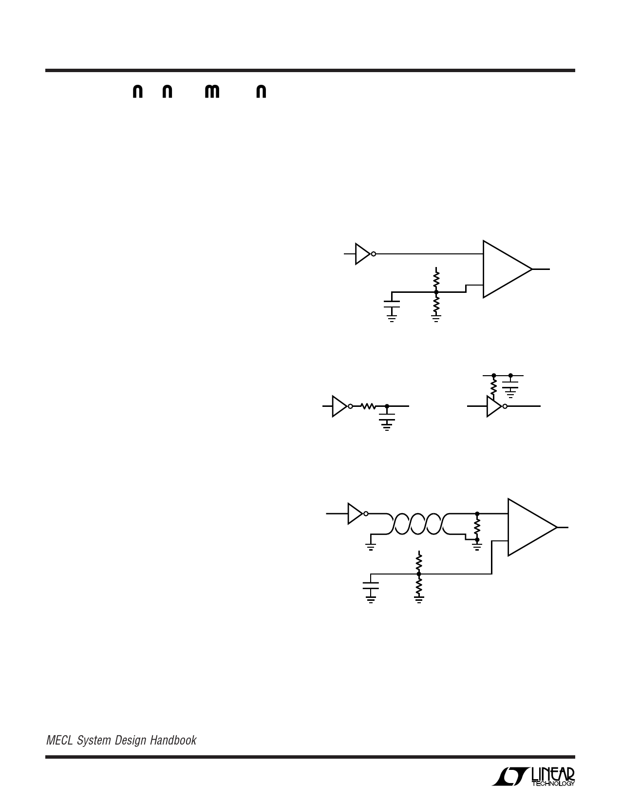
Single-Ended Applications
Over short distances, the LTC1520 can be configured to
receive single-ended data by tying one input to a fixed bias
voltage and connecting the other input to the driver output.
In such applications, standard high speed CMOS logic
may be used as a driver for the LTC1520. The receiver trip
points may be easily adjusted to accommodate different
driver output swings by changing the resistor divider at the
fixed input. Figure 6a shows a single-ended receiver
configuration with the driver and receiver connected via
PC traces. Note that at very high speeds, transmission line
and driver ringing effects have to be considered. Motorola’s
MECL System Design Handbook serves as an excellent
reference for transmission line and termination effects. To
mitigate transmission errors and duty cycle distortion due
to driver ringing, a small output filter or a dampening
resistor on VDD may be needed as shown in Figure 6b. To
transmit single-ended data over distances up to 10 feet,
twisted pair is recommended with the unused wire
grounded at both ends (Figure 7).
MC74ACT04
(TTL INPUT)
MC74AC04
(CMOS INPUT)
PC TRACE
5V
2.2k
0.01µF
2.2k
–
1/4 LTC1520
+
1520 F06a
Figure 6a. Single-Ended Receiver
MC74AC04
10Ω
10Ω
PC TRACE OR
10pF
0.01µF
PC TRACE
1520 F06b
Figure 6b. Techniques to Minimize Driver Ringing
MC74ACT04
MC74AC04
10-FT TWISTED PAIR
5V
3.3k
120Ω
–
1/4 LTC1520
+
0.01µF
2.2k
1520 F07
Figure 7. Medium Distance Single-Ended Transmission
Using a CMOS Driver
Differential Transmission
The LTC1520 is well suited for medium distance differen-
tial transmission due to its rail-to-rail input common mode
range. Clock rates up to 25MHz can be transmitted over
100 feet of high quality twisted pair. Figure 8 shows the
6
Share Link: 