LTC1628CG-SYNC 查看數據表(PDF) - Linear Technology
零件编号
产品描述 (功能)
生产厂家
LTC1628CG-SYNC Datasheet PDF : 32 Pages
| |||
LTC1628-SYNC
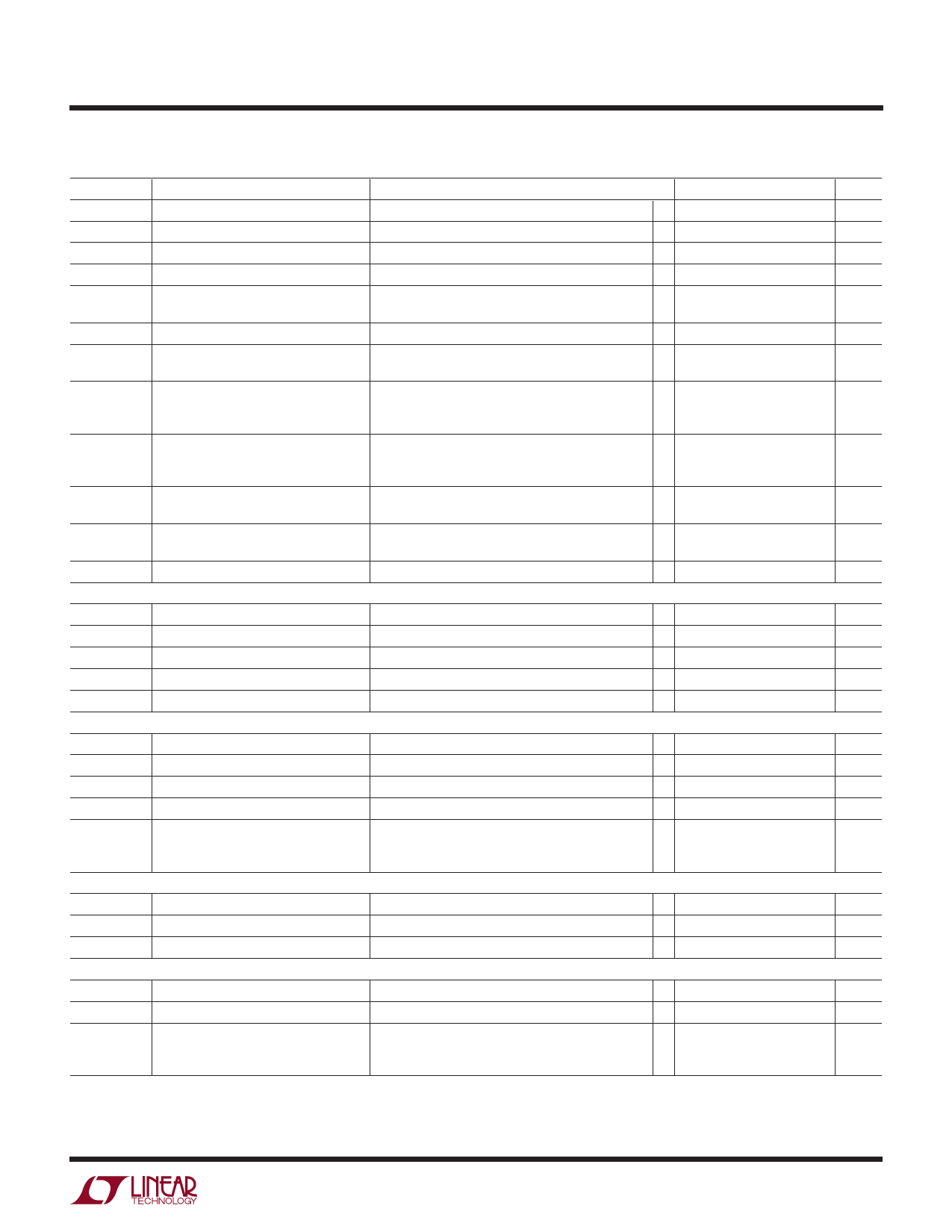
ELECTRICAL CHARACTERISTICS The q denotes the specifications which apply over the full operating
temperature range, otherwise specifications are at TA = 25°C. VIN = 15V, VRUN/SS1, 2 = 5V unless otherwise noted.
SYMBOL
PARAMETER
CONDITIONS
MIN TYP MAX UNITS
DFMAX
Maximum Duty Factor
In Dropout
IRUN/SS1, 2
Soft-Start Charge Current
VRUN/SS1, 2 = 1.9V
VRUN/SS1, 2 ON RUN/SS Pin ON Threshold
VRUN/SS1, VRUN/SS2 Rising
VRUN/SS1, 2 LT RUN/SS Pin Latchoff Arming Threshold VRUN/SS1, VRUN/SS2 Rising from 3V
ISCL1, 2
RUN/SS Discharge Current
Soft Short Condition VOSENSE1, 2 = 0.5V;
VRUN/SS1, 2 = 4.5V
ISDLHO
Shutdown Latch Disable Current
VOSENSE1, 2 = 0.5V
VSENSE(MAX) Maximum Current Sense Threshold
VOSENSE1, 2 = 0.7V,VSENSE1–, 2 – = 5V
VOSENSE1, 2 = 0.7V,VSENSE1–, 2 – = 5V
TG1, 2 tr
TG1, 2 tf
TG Transition Time:
Rise Time
Fall Time
(Note 5)
CLOAD = 3300pF
CLOAD = 3300pF
BG1, 2 tr
BG1, 2 tf
BG Transition Time:
Rise Time
Fall Time
(Note 5)
CLOAD = 3300pF
CLOAD = 3300pF
TG/BG t1D
Top Gate Off to Bottom Gate On Delay
Synchronous Switch-On Delay Time CLOAD = 3300pF Each Driver
BG/TG t2D
Bottom Gate Off to Top Gate On Delay
Top Switch-On Delay Time
CLOAD = 3300pF Each Driver
tON(MIN)
Minimum On-Time
Tested with a Square Wave (Note 6)
INTVCC Linear Regulator
VINTVCC
Internal VCC Voltage
6V < VIN < 30V, VEXTVCC = 4V
VLDO INT
INTVCC Load Regulation
ICC = 0 to 20mA, VEXTVCC = 4V
VLDO EXT
EXTVCC Voltage Drop
ICC = 20mA, VEXTVCC = 5V
VEXTVCC
EXTVCC Switchover Voltage
ICC = 20mA, EXTVCC Ramping Positive
VLDOHYS
EXTVCC Hysteresis
Oscillator and Phase-Locked Loop
98
99.4
%
0.5
1.2
µA
1.0
1.5
1.9
V
4.1
4.5
V
0.5
2
4
µA
1.6
5
µA
65
75
85
mV
q 62
75
88
mV
50
90
ns
50
90
ns
40
90
ns
40
80
ns
90
ns
90
ns
180
ns
4.8
5.0
5.2
V
0.2
1.0
%
80
160
mV
q 4.5
4.7
V
0.2
V
fNOM
fLOW
fHIGH
RPLLIN
IPLLFLTR
Nominal Frequency
Lowest Frequency
Highest Frequency
PLLIN Input Resistance
Phase Detector Output Current
Sinking Capability
Sourcing Capability
3.3V Linear Regulator
VPLLFLTR = 1.2V
VPLLFLTR = 0V
VPLLFLTR ≥ 2.4V
fPLLIN < fOSC
fPLLIN > fOSC
190 220 250
kHz
120 140 160
kHz
280 310 360
kHz
50
kΩ
–15
µA
15
µA
V3.3OUT
3.3V Regulator Output Voltage
V3.3IL
3.3V Regulator Load Regulation
V3.3VL
3.3V Regulator Line Regulation
PGOOD Output
No Load
I3.3 = 0 to 10mA
6V < VIN < 30V
q 3.25 3.35 3.45
V
0.5
2
%
0.05
0.2
%
VPGL
IPGOOD
VPG
PGOOD Voltage Low
PGOOD Leakage Current
PGOOD Trip Level, Either Controller
IPGOOD = 2mA
VPGOOD = 5V
VOSENSE with Respect to Set Output Voltage
VOSENSE Ramping Negative
VOSENSE Ramping Positive
0.1
0.3
V
±1
µA
–6
–7.5 – 9.5
%
6
7.5
9.5
%
3
Share Link: 