LTC1700EMS 查看數據表(PDF) - Linear Technology
零件编号
产品描述 (功能)
生产厂家
LTC1700EMS Datasheet PDF : 16 Pages
| |||
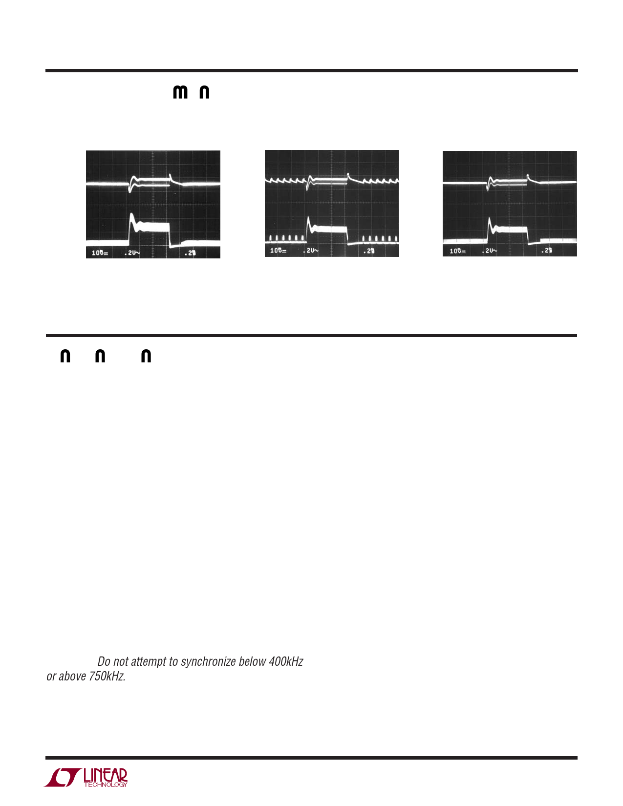
TYPICAL PERFORMANCE CHARACTERISTICS
LTC1700
Load Step Transient Response
Burst Mode Operation Inhibited
Load Step Transient Response
Burst Mode Operation Enabled
Load Step Transient Response
Burst Mode Operation Inhibited
A/C COUPLED
OUTPUT
VOLTAGE
(0.2V/DIV)
INDUCTOR
CURRENT
(2A/DIV)
A/C COUPLED
OUTPUT
VOLTAGE
(0.2V/DIV)
INDUCTOR
CURRENT
(2A/DIV)
A/C COUPLED
OUTPUT
VOLTAGE
(0.2V/DIV)
INDUCTOR
CURRENT
(2A/DIV)
VIN = 3.3V
VOUT = 5V
2A/DIV
1700 G13
VSYNC = 0V
LOAD STEP = 100mA TO 1.7A
VIN = 4.2V
VOUT = 5V
2A/DIV
1700 G14
VSYNC = VIN
LOAD STEP = 100mA TO 1.7A
VIN = 4.2V
VOUT = 5V
2A/DIV
1700 G15
VSYNC = 0V
LOAD STEP = 100mA TO 1.7A
PIN FUNCTIONS
SGND (Pin 1): Small-Signal Ground. Must be routed
separately from other grounds to the (–) terminal of COUT.
ITH (Pin 2): Error Amplifier Compensation Point. The
current comparator threshold increases with this control
voltage. Nominal voltage range for this pin is 0V to 1.18V.
VFB (Pin 3): Receives the feedback voltage from an exter-
nal resistive divider across the output capacitor.
RUN/SS (Pin 4): Combination of Soft-Start and Run
Control Inputs. A capacitor to ground at this pin sets the
ramp time to full output current. The time is approximately
0.45s/µF. Forcing this pin below 1.08V causes all circuitry
to be shut down.
SYNC/MODE (Pin 5): This pin performs three functions. A
voltage greater than 1.2V on this pin allows Burst Mode
operation at low load currents, while grounding or apply-
ing a clock signal on this pin defeats Burst Mode operation.
An external clock between 400kHz and 750kHz applied to
this pin forces the LTC1700 to operate at the external clock
frequency. Do not attempt to synchronize below 400kHz
or above 750kHz.
TG (Pin 6): Top Gate Drive. Drives the external synchro-
nous P-channel MOSFET with a voltage swing between 0V
to VOUT.
VOUT (Pin 7): This pin performs two functions. It serves as
the supply pin and also as one of the inputs to the current
reversal comparator.
BG (Pin 8): Bottom Gate Drive. Drives the external main
N-channel MOSFET with a voltage swing between 0V to
VOUT.
PGND (Pin 9): Top and Bottom Gate Drivers Ground.
Connects to the (–) terminal of COUT. Source of the main
N-channel MOSFET must be connected close to this pin
since this pin is also one of the inputs to the VDS sense
amplifier.
SW (Pin 10): This pin connects to the inputs of two
comparators: The VDS sense amplifier and the current
reversal comparator. The drain of an internal N-channel
start-up MOSFET (M1) is also connected to this pin.
1700fa
5
Share Link: 