LTC1751-5 查看數據表(PDF) - Linear Technology
零件编号
产品描述 (功能)
生产厂家
LTC1751-5 Datasheet PDF : 12 Pages
| |||
LTC1751/LTC1751-3.3/LTC1751-5
APPLICATIO S I FOR ATIO
Programming the LTC1751 Output Voltage (FB Pin)
While the LTC1751-3.3/LTC1751-5 versions have internal
resistive dividers to program the output voltage, the
programmable LTC1751 may be set to an arbitrary voltage
via an external resistive divider. Since it employs a voltage
doubling charge pump, it is not possible to achieve output
voltages greater than twice the available input voltage.
Figure 3 shows the required voltage divider connection.
The voltage divider ratio is given by the expression:
R1 = VOUT – 1
R2 1.205V
2
VOUT
R1
1
FB
R2
4
GND
1751 F03
( ) VOUT
1.205V 1 + R1
R2
COUT
Figure 3. Programming the Adjustable LTC1751
The sum of the voltage divider resistors can be made large
to keep the quiescent current to a minimum. Any standing
current in the output divider (given by 1.205V/R2) will be
reflected by a factor of 2 in the input current. Typical values
for total voltage divider resistance can range from several
kΩs up to 1MΩ.
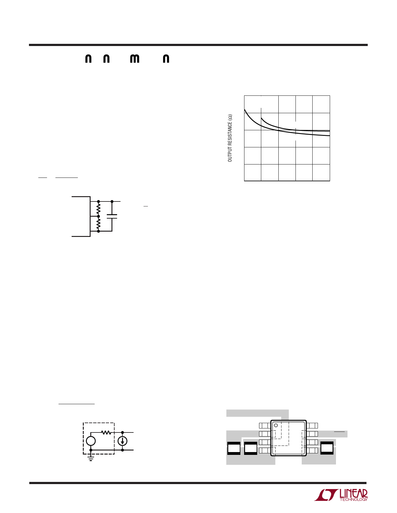
Maximum Available Output Current
For the adjustable LTC1751, the maximum available out-
put current and voltage can be calculated from the effec-
tive open-loop output resistance, ROUT, and effective
output voltage, 2VIN(MIN).
From Figure 4 the available current is given by:
IOUT
=
2VIN – VOUT
ROUT
ROUT
+
+– 2VIN
VOUT
–
1751 F04
Figure 4. Equivalent Open-Loop Circuit
Typical ROUT values as a function of input voltage are
shown in Figure 5.
10
TA = 25°C
CFLY = 1µF
8
IOUT = 100mA
6
IOUT = 50mA
4
2
0
2.0 2.5 3.0 3.5 4.0 4.5
INPUT VOLTAGE (V)
1751 F05
Figure 5. Typical ROUT vs Input Voltage
Layout Considerations
Due to high switching frequency and high transient cur-
rents produced by the LTC1751 product family, careful
board layout is necessary. A true ground plane and short
connections to all capacitors will improve performance and
ensure proper regulation under all conditions. Figure 6
shows the recommended layout configuration.
Thermal Management
For higher input voltages and maximum output current,
there can be substantial power dissipation in the
LTC1751. If the junction temperature increases above
approximately 160°C, the thermal shutdown circuitry
will automatically deactivate the output. To reduce the
maximum junction temperature, a good thermal connec-
tion to the PC board is recommended. Connecting the
GND pin (Pin 4) to a ground plane, and maintaining a
solid ground plane under the device on two layers of the
PC board, will reduce the thermal resistance of the
package and PC board system considerably.
VIN
VOUT
SHDN
GND
17515 F03
Figure 6. Recommended Layout
10
Share Link: 