LTC1700_ 查看數據表(PDF) - Linear Technology
零件编号
产品描述 (功能)
生产厂家
LTC1700_ Datasheet PDF : 32 Pages
| |||
LTC1871-7
U
OPERATIO
Attempting to synchronize to too high an external fre-
quency (above 1.3fO) can result in inadequate slope com-
pensation and possible subharmonic oscillation (or jitter).
The external clock signal must exceed 2V for at least 25ns,
and should have a maximum duty cycle of 80%, as shown
in Figure 5. The MOSFET turn on will synchronize to the
rising edge of the external clock signal.
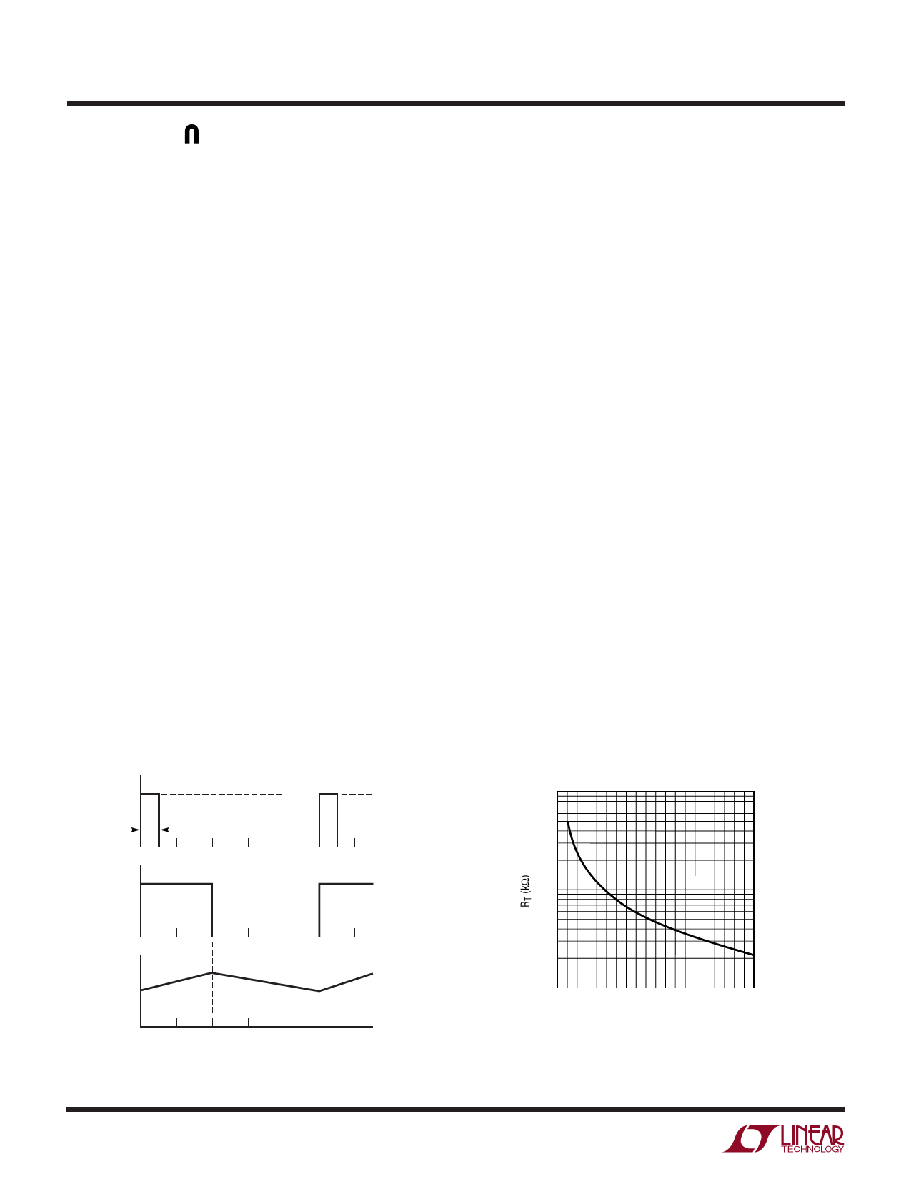
Programming the Operating Frequency
The choice of operating frequency and inductor value is a
tradeoff between efficiency and component size. Low
frequency operation improves efficiency by reducing
MOSFET and diode switching losses. However, lower
frequency operation requires more inductance for a given
amount of load current.
The LTC1871-7 uses a constant frequency architecture
that can be programmed over a 50kHz to 1000kHz range
with a single external resistor from the FREQ pin to
ground, as shown in Figure 1. The nominal voltage on the
FREQ pin is 0.6V, and the current that flows into the FREQ
pin is used to charge and discharge an internal oscillator
capacitor. A graph for selecting the value of RT for a given
operating frequency is shown in Figure 6.
INTVCC Regulator Bypassing and Operation
An internal, P-channel low dropout voltage regulator pro-
duces the 7V supply which powers the gate driver and
MODE/
SYNC
GATE
tMIN = 25ns
2V TO 7V
0.8T T T = 1/fO
D = 40%
logic circuitry within the LTC1871-7, as shown in Figure 7.
The INTVCC regulator can supply up to 50mA and must be
bypassed to ground immediately adjacent to the IC pins
with a minimum of 4.7µF tantalum or ceramic capacitor.
Good bypassing is necessary to supply the high transient
currents required by the MOSFET gate driver.
The LTC1871-7 contains an undervoltage lockout circuit
which protects the external MOSFET from switching at low
gate-to-source voltages. This undervoltage circuit senses
the INTVCC voltage and has a 5.6V rising threshold and a
4.6V falling threshold.
For input voltages that don’t exceed 8V (the absolute
maximum rating for INTVCC is 9V), the internal low drop-
out regulator in the LTC1871-7 is redundant and the
INTVCC pin can be shorted directly to the VIN pin. With the
INTVCC pin shorted to VIN, however, the divider that
programs the regulated INTVCC voltage will draw 14µA of
current from the input supply, even in shutdown mode.
For applications that require the lowest shutdown mode
input supply current, do not connect the INTVCC pin to VIN.
Regardless of whether the INTVCC pin is shorted to VIN or
not, it is always necessary to have the driver circuitry
bypassed with a 4.7µF ceramic capacitor to ground
immediately adjacent to the INTVCC and GND pins.
In an actual application, most of the IC supply current is
used to drive the gate capacitance of the power MOSFET.
As a result, high input voltage applications in which a large
power MOSFET is being driven at high frequencies can
1000
100
IL
18717 F05
Figure 5. MODE/SYNC Clock Input and Switching
Waveforms for Synchronized Operation
10
10
0 100 200 300 400 500 600 700 800 900 1000
FREQUENCY (kHz)
18717 F06
Figure 6. Timing Resistor (RT) Value
18717f
Share Link: 