LTC1700_ 查看數據表(PDF) - Linear Technology
零件编号
产品描述 (功能)
生产厂家
LTC1700_ Datasheet PDF : 32 Pages
| |||
LTC1871-7
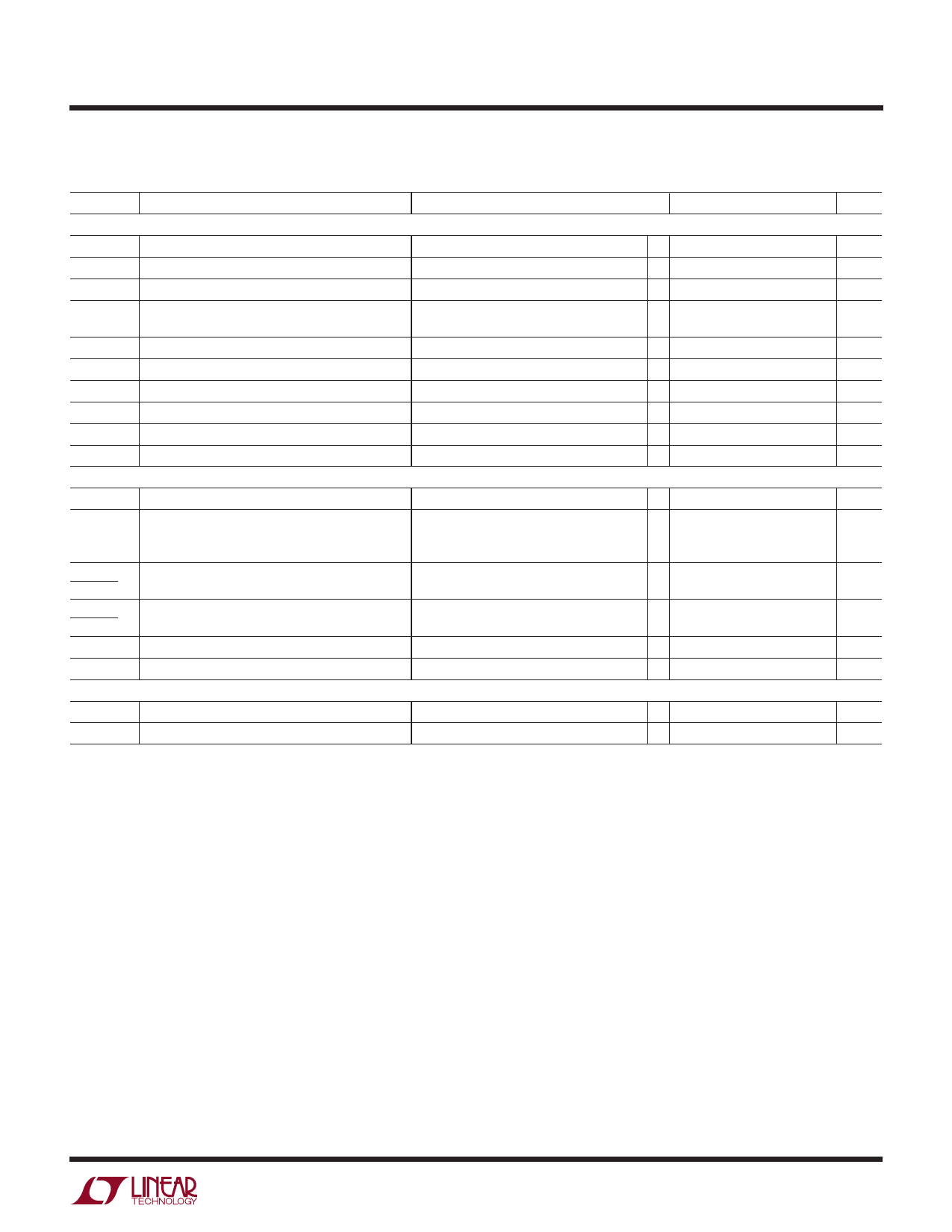
ELECTRICAL CHARACTERISTICS
The q denotes specifications which apply over the full operating temperature range, otherwise specifications are at TA = 25°C.
VIN = 8V, VRUN = 1.5V, RFREQ = 80k, VMODE/SYNC = 0V, unless otherwise specified.
SYMBOL PARAMETER
CONDITIONS
MIN TYP MAX UNITS
Oscillator
fOSC
Oscillator Frequency
Oscillator Frequency Range
RFREQ = 80k
250 300 350
kHz
50
1000
kHz
DMAX
fSYNC/fOSC
Maximum Duty Cycle
Recommended Maximum Synchronized
Frequency Ratio
fOSC = 300kHz (Note 6)
87
92
97
%
1.25 1.30
tSYNC(MIN) MODE/SYNC Minimum Input Pulse Width
tSYNC(MAX) MODE/SYNC Maximum Input Pulse Width
VIL(MODE) Low Level MODE/SYNC Input Voltage
VIH(MODE) High Level MODE/SYNC Input Voltage
RMODE/SYNC MODE/SYNC Input Pull-Down Resistance
VFREQ
Nominal FREQ Pin Voltage
Low Dropout Regulator
VSYNC = 0V to 5V
VSYNC = 0V to 5V
25
ns
0.8/fOSC
ns
0.3
V
1.2
V
50
kΩ
0.62
V
VINTVCC
UVLO
INTVCC Regulator Output Voltage
INTVCC Undervoltage Lockout Thresholds
∆VINTVCC
∆VIN1
∆VINTVCC
∆VIN2
VLDO(LOAD)
VDROPOUT
GATE Driver
INTVCC Regulator Line Regulation
INTVCC Regulator Line Regulation
INTVCC Load Regulation
INTVCC Regulator Dropout Voltage
VIN = 8V
Rising INTVCC
Falling INTVCC
UVLO Hysteresis
8V ≤ VIN ≤ 15V
15V ≤ VIN ≤ 30V
0 ≤ IINTVCC ≤ 20mA, VIN = 8V
VIN = 6V, INTVCC Load = 20mA
6.5
7
7.5
V
5.6
V
4.6
V
1.0
V
8
25
mV
70
200
mV
–2
– 0.2
%
280
mV
tr
GATE Driver Output Rise Time
tf
GATE Driver Output Fall Time
CL = 3300pF (Note 7)
CL = 3300pF (Note 7)
17
100
ns
8
100
ns
Note 1: Absolute Maximum Ratings are those values beyond which the life
of the device may be impaired.
Note 2: The LTC1871-7E is guaranteed to meet performance specifications
from 0°C to 70°C. Specifications over the – 40°C to 85°C operating
temperature range are assured by design, characterization and correlation
with statistical process controls.
Note 3: TJ is calculated from the ambient temperature TA and power
dissipation PD according to the following formula:
TJ = TA + (PD • 120°C/W)
Note 4: The dynamic input supply current is higher due to power MOSFET
gate charging (QG • fOSC). See Applications Information.
Note 5: The LTC1871-7 is tested in a feedback loop that servos VFB to the
reference voltage with the ITH pin forced to a voltage between 0V and 1.4V
(the no load to full load operating voltage range for the ITH pin is 0.3V to
1.23V).
Note 6: In a synchronized application, the internal slope compensation
gain is increased by 25%. Synchronizing to a significantly higher ratio will
reduce the effective amount of slope compensation, which could result in
subharmonic oscillation for duty cycles greater than 50%.
Note 7: Rise and fall times are measured at 10% and 90% levels.
18717f
3
Share Link: 