LTC1700_ 查看數據表(PDF) - Linear Technology
零件编号
产品描述 (功能)
生产厂家
LTC1700_ Datasheet PDF : 32 Pages
| |||
LTC1871-7
U
OPERATIO
Main Control Loop
The LTC1871-7 is a constant frequency, current mode
controller for DC/DC boost, SEPIC and flyback converter
applications. With the LTC1871-7 the current control loop
can be closed by sensing the voltage drop either across the
power MOSFET switch or across a discrete sense resistor,
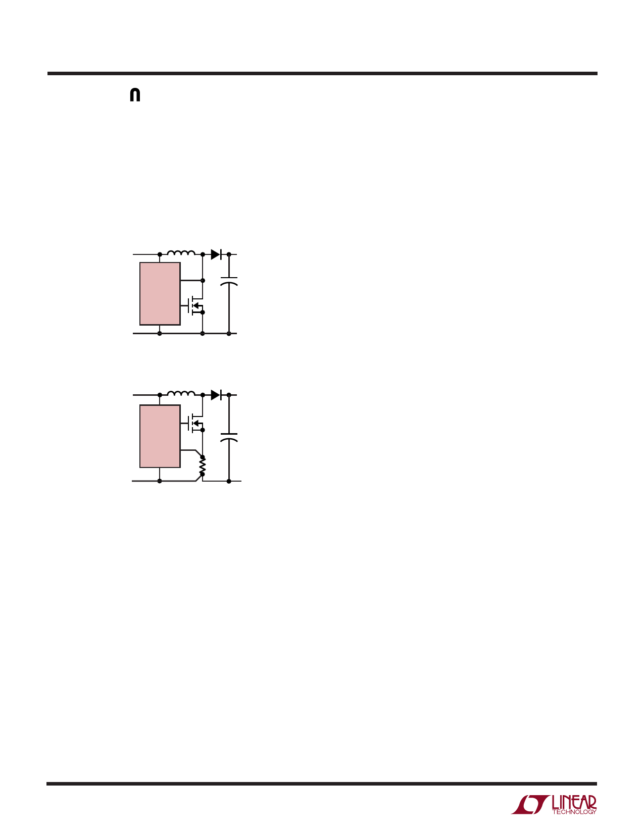
as shown in Figure 2.
L
D
VIN
VOUT
VIN
SENSE
+
VSW
COUT
GATE
GND
GND
2a. SENSE Pin Connection for
Maximum Efficiency (VSW < 36V)
L
D
VIN
VOUT
VIN
GATE
SENSE
GND
VSW
+
COUT
RS
GND
18717 F02
2b. SENSE Pin Connection for Precise
Control of Peak Current or for VSW > 36V
Figure 2. Using the SENSE Pin On the LTC1871-7
For circuit operation, please refer to the Block Diagram of
the IC and Figure 1. In normal operation, the power
MOSFET is turned on when the oscillator sets the PWM
latch and is turned off when the current comparator C1
resets the latch. The divided-down output voltage is com-
pared to an internal 1.230V reference by the error amplifier
EA, which outputs an error signal at the ITH pin. The voltage
on the ITH pin sets the current comparator C1 input
threshold. When the load current increases, a fall in the FB
voltage relative to the reference voltage causes the ITH pin
to rise, which causes the current comparator C1 to trip at
a higher peak inductor current value. The average inductor
current will therefore rise until it equals the load current,
thereby maintaining output regulation.
8
The nominal operating frequency of the LTC1871-7 is
programmed using a resistor from the FREQ pin to ground
and can be controlled over a 50kHz to 1000kHz range. In
addition, the internal oscillator can be synchronized to an
external clock applied to the MODE/SYNC pin and can be
locked to a frequency between 100% and 130% of its
nominal value. When the MODE/SYNC pin is left open, it is
pulled low by an internal 50k resistor and Burst Mode
operation is enabled. If this pin is taken above 2V or an
external clock is applied, Burst Mode operation is disabled
and the IC operates in continuous mode. With no load (or
an extremely light load), the controller will skip pulses in
order to maintain regulation and prevent excessive output
ripple.
The RUN pin controls whether the IC is enabled or is in a
low current shutdown state. A micropower 1.248V refer-
ence and comparator C2 allow the user to program the
supply voltage at which the IC turns on and off (compara-
tor C2 has 100mV of hysteresis for noise immunity). With
the RUN pin below 1.248V, the chip is off and the input
supply current is typically only 10µA.
An overvoltage comparator OV senses when the FB pin
exceeds the reference voltage by 6.5% and provides a
reset pulse to the main RS latch. Because this RS latch is
reset-dominant, the power MOSFET is actively held off for
the duration of an output overvoltage condition.
The LTC1871-7 can be used either by sensing the voltage
drop across the power MOSFET or by connecting the
SENSE pin to a conventional shunt resistor in the source
of the power MOSFET, as shown in Figure 2. Sensing the
voltage across the power MOSFET maximizes converter
efficiency and minimizes the component count, but limits
the output voltage to the maximum rating for this pin
(36V). By connecting the SENSE pin to a resistor in the
source of the power MOSFET, the user is able to program
output voltages significantly greater than 36V.
Programming the Operating Mode
For applications where maximizing the efficiency at very
light loads (e.g., <100µA) is a high priority, the current in
the output divider could be decreased to a few micro-
amps and Burst Mode operation should be applied (i.e.,
the MODE/SYNC pin should be connected to ground).
18717f
Share Link: 