LTC1700_ 查看數據表(PDF) - Linear Technology
零件编号
产品描述 (功能)
生产厂家
LTC1700_ Datasheet PDF : 32 Pages
| |||
U
OPERATIO
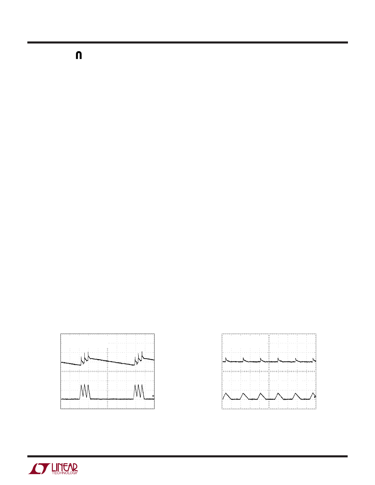
In applications where fixed frequency operation is more
critical than low current efficiency, or where the lowest
output ripple is desired, pulse-skip mode operation should
be used and the MODE/SYNC pin should be connected to
the INTVCC pin. This allows discontinuous conduction
mode (DCM) operation down to near the limit defined by
the chip’s minimum on-time (about 175ns). Below this
output current level, the converter will begin to skip
cycles in order to maintain output regulation. Figures 3
and 4 show the light load switching waveforms for Burst
Mode and pulse-skip mode operation for the converter in
Figure␣ 1.
Burst Mode Operation
Burst Mode operation is selected by leaving the MODE/
SYNC pin unconnected or by connecting it to ground. In
normal operation, the range on the ITH pin corresponding
to no load to full load is 0.30V to 1.2V. In Burst Mode
operation, if the error amplifier EA drives the ITH voltage
below 0.525V, the buffered ITH input to the current
comparator C1 will be clamped at 0.525V (which corre-
sponds to 25% of maximum load current). The inductor
current peak is then held at approximately 30mV divided
by the power MOSFET RDS(ON). If the ITH pin drops below
0.30V, the Burst Mode comparator B1 will turn off the
power MOSFET and scale back the quiescent current of
the IC to 250µA (sleep mode). In this condition, the load
current will be supplied by the output capacitor until the
ITH voltage rises above the 50mV hysteresis of the burst
comparator. At light loads, short bursts of switching
LTC1871-7
(where the average inductor current is 20% of its maxi-
mum value) followed by long periods of sleep will be
observed, thereby greatly improving converter efficiency.
Oscilloscope waveforms illustrating Burst Mode opera-
tion are shown in Figure 3.
Pulse-Skip Mode Operation
With the MODE/SYNC pin tied to a DC voltage above 2V,
Burst Mode operation is disabled. The internal, 0.525V
buffered ITH burst clamp is removed, allowing the ITH pin
to directly control the current comparator from no load to
full load. With no load, the ITH pin is driven below 0.30V,
the power MOSFET is turned off and sleep mode is
invoked. Oscilloscope waveforms illustrating this mode of
operation are shown in Figure 4.
When an external clock signal drives the MODE/SYNC pin
at a rate faster than the chip’s internal oscillator, the
oscillator will synchronize to it. In this synchronized mode,
Burst Mode operation is disabled. The constant frequency
associated with synchronized operation provides a more
controlled noise spectrum from the converter, at the
expense of overall system efficiency of light loads.
When the oscillator’s internal logic circuitry detects a
synchronizing signal on the MODE/SYNC pin, the internal
oscillator ramp is terminated early and the slope compen-
sation is increased by approximately 30%. As a result, in
applications requiring synchronization, it is recommended
that the nominal operating frequency of the IC be pro-
grammed to be about 75% of the external clock frequency.
MODE/SYNC = 0V
(Burst Mode OPERATION)
VOUT
50mV/DIV
MODE/SYNC = INTVCC
(PULSE SKIP MODE)
VOUT
50mV/DIV
IL
5A/DIV
10µs/DIV
18717 F03
Figure 3. LTC1871-7 Burst Mode Operation
(MODE/SYNC = 0V) at Low Output Current
IL
5A/DIV
2µs/DIV
18717 F04
Figure 4. LTC1871-7 Low Output Current Operation with
Burst Mode Operation Disabled (MODE/SYNC = INTVCC)
18717f
9
Share Link: 