LTC2053IMS8(RevB) 查看數據表(PDF) - Linear Technology
零件编号
产品描述 (功能)
生产厂家
LTC2053IMS8
(Rev.:RevB)
(Rev.:RevB)
Linear Technology

LTC2053IMS8 Datasheet PDF : 16 Pages
| |||
LTC2053/LTC2053-SYNC
APPLICATIO S I FOR ATIO
Synchronizing to an External Clock
(LTC2053-SYNC Only)
The LTC2053 has an internally generated sample clock
that is typically 3kHz. There is no need to provide the
LTC2053 with a clock. However, in some applications, it
may be desirable for the user to control the sampling
frequency more precisely to avoid undesirable aliasing.
This can be done with the LTC2053-SYNC. This device
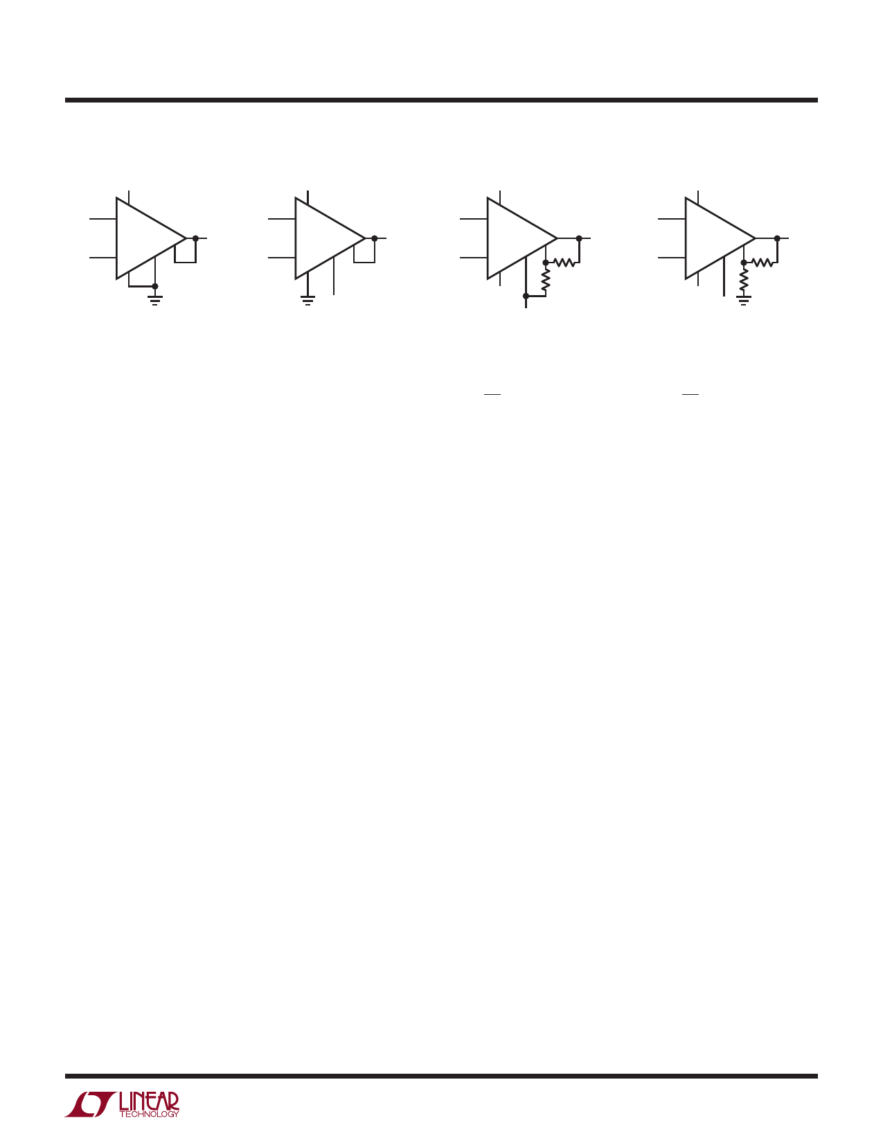
uses PIN 1 as a clock input whereas the LTC2053 uses Pin
1 as an enable pin. If CLK (PIN 1) is left floating on the
LTC2053-SYNC, the device will run on its internal oscilla-
tor, similar to the LTC2053. However, if not externally
synchronizing to a system clock, it is recommended that
the LTC2053 be used instead of the LTC2053-SYNC
because the LTC2053-SYNC is sensitive to parasitic ca-
pacitance on the CLK pin when left floating. Clocking the
LTC2053-SYNC is accomplished by driving the CLK pin
at 8 times the desired sample clock frequency. This
completely disables the internal clock. For example, to
achieve the nominal LTC2053 sample clock rate of 3kHz,
a 24kHz external clock should be applied to the CLK pin
of the LTC2053-SYNC. If a square wave is used to drive the
CLK pin, a 5µs RC time constant should be placed in front
of the CLK pin to maintain low offset voltage performance
(see Figure 2). This avoids internal and external coupling
of the high frequency components of the external clock at
the instant the LTC2053-SYNC holds the sampled input.
The LTC2053-SYNC is tested with a sample clock of 3kHz
(fCLK = 24kHz) to the same specifications as the LTC2053.
In addition the LTC2053-SYNC is tested at 1/2 and 2X this
frequency to verify proper operation. The curves in the
Typical Performance Characteristics section of this
datasheet apply to the LTC2053-SYNC when driving it with
a 24kHz clock at PIN1 (fCLK = 24kHz, 3kHz sample clock
rate). Below are three curves that show the behavior of the
LTC2053-SYNC as the clock frequency is varied. The
offset is essentially unaffected over a 2:1 increase or
decrease of the typical LTC2053 sample clock speed. The
bias current is directly proportional to the clock speed. The
noise is roughly proportional to the square root of the
clock frequency. For optimum noise and bias current
performance, drive the LTC2053-SYNC with a nominal
24kHz external clock (3kHz sample clock).
5V
8
V+IN + 3 +
1
VD
CLK
V–IN – 2 –
5
LTC2053-SYNC 4
7
6 R2
R1
1kΩ EXTERNAL
CLOCK
4.7nF
5V
0V
VOUT
Figure 2
2053 F02
20
15
10
5
0
–5
–10
–15
–20
0
LTC2053-SYNC
Input Offset
vs Sample Frequency
VS = ±5V
VS = 5V
VS = 3V
Typ LTC2053 Sample Frequency
2000 4000 6000 8000 10000
SAMPLE FREQUENCY (Hz) (=FCLK/8)
2053 F03
LTC2053-SYNC
Average Input Bias Current
vs Sample Frequency
14
VS = 5V
12
VREF = 0
VCM = 1V
10
8
6
4
Typ LTC2053 Sample Frequency
2
0
0 2000 4000 6000 8000 10000
SAMPLE FREQUENCY (Hz) (=FCLK/8)
2053 F04
LTC2053-SYNC
Input Referred Noise
vs Sample Frequency
12
VS = 5V
TA = 25°C
10
Noise in 10Hz Bandwidth
8
Typ LTC2053 Sample Frequency
6
4
2
0
0 2000 4000 6000 8000 10000
SAMPLE FREQUENCY (FCLK/8)
2053 F05
2053syncfb
11
Share Link: