LTC2053IMS8 查看數據表(PDF) - Linear Technology
零件编号
产品描述 (功能)
生产厂家
LTC2053IMS8
Linear Technology

LTC2053IMS8 Datasheet PDF : 18 Pages
| |||
LTC2053/LTC2053-SYNC
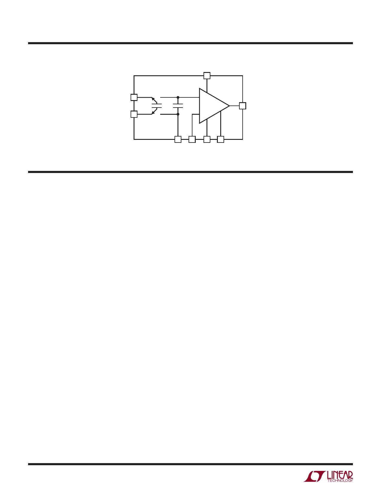
Block Diagram
+IN
3
–IN
2
8
V+
ZERO-DRIFT
+ OP AMP
CS
CH
OUT 7
–
REF RG V– EN/CLK*
5
6
4
1
2053 BD
*NOTE: PIN 1 IS EN ON THE LTC2053 AND CLK ON THE LTC2053-SYNC
Applications Information
Theory of Operation
The LTC2053 uses an internal capacitor (CS) to sample
a differential input signal riding on a DC common mode
voltage (see the Block Diagram). This capacitor’s charge is
transferred to a second internal hold capacitor (CH) trans-
lating the common mode of the input differential signal to
that of the REF pin. The resulting signal is amplified by a
zero-drift op amp in the noninverting configuration. The
RG pin is the negative input of this op amp and allows
external programmability of the DC gain. Simple filtering
can be realized by using an external capacitor across the
feedback resistor.
Input Voltage Range
The input common mode voltage range of the LTC2053
is rail-to-rail. However, the following equation limits the
size of the differential input voltage:
V– ≤ (V+IN – V–IN) + VREF ≤ V+ – 1.3
Where V+IN and V–IN are the voltages of the +IN and –IN
pins, respectively, VREF is the voltage at the REF pin and
V+ is the positive supply voltage.
For example, with a 3V single supply and a 0V to 100mV
differential input voltage, VREF must be between 0V and
1.6V.
±5 Volt Operation
When using the LTC2053 with supplies over 5.5V, care
must be taken to limit the maximum difference between
any of the input pins (+IN or –IN) and the REF pin to
5.5V; if not, the device will be damaged. For example, if
rail-to-rail input operation is desired when the supplies
are at ±5V, the REF pin should be 0V, ±0.5V. As a second
example, if V+ is 10V and V– and REF are at 0V, the inputs
should not exceed 5.5V.
Settling Time
The sampling rate is 3kHz and the input sampling period
during which CS is charged to the input differential voltage
VIN is approximately 150µs. First assume that on each
input sampling period, CS is charged fully to VIN. Since
CS = CH (= 1000pF), a change in the input will settle to
N bits of accuracy at the op amp noninverting input after
N clock cycles or 333µs(N). The settling time at the OUT
pin is also affected by the settling of the internal op amp.
Since the gain bandwidth of the internal op amp is typically
200kHz, the settling time is dominated by the switched
capacitor front end for gains below 100 (see the Typical
Performance Characteristics section).
10
2053syncfc
Share Link: