LTC2053IMS8 查看數據表(PDF) - Linear Technology
零件编号
产品描述 (功能)
生产厂家
LTC2053IMS8
Linear Technology

LTC2053IMS8 Datasheet PDF : 18 Pages
| |||
LTC2053/LTC2053-SYNC
Applications Information
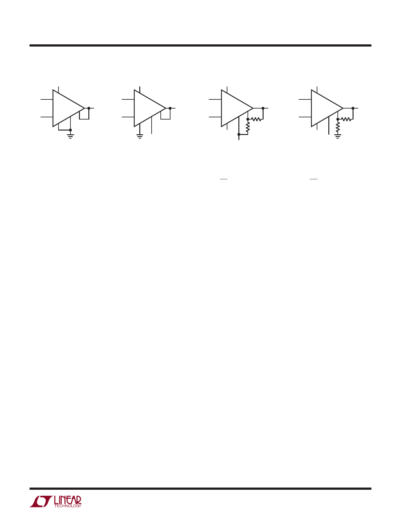
SINGLE SUPPLY, UNITY GAIN
5V
8
V+IN
3
+
+
V–IN V–IN 2 –
4
7
6
5
VOUT
SINGLE SUPPLY, UNITY GAIN
5V
8
V+IN
3
+
+
V–IN V–IN 2 –
4
7
6
5
VOUT
VREF
DUAL SUPPLY, NONUNITY GAIN
5V
8
V+IN
3
+
+
V–IN V–IN 2 –
4
–5V
7
6 R2
5
R1
VOUT
VREF
DUAL SUPPLY, NONUNITY GAIN
5V
8
V+IN + 3 +
V–IN V–IN 2 –
5
4
–5V VREF
7
6 R2
R1
VOUT
0V < V+IN < 5V
0V < V–IN < 5V
0V < VIN < 3.7V
VOUT = VIN
0V < V–IN < 5V AND |V–IN – VREF| < 5.5V
0V < V+IN < 5V AND |V+IN – VREF| < 5.5V
0V < VIN + VREF < 3.7V
VOUT = VIN + VREF
–5V < V–IN < 5V AND |V–IN – VREF| < 5.5V
–5V < V+IN < 5V AND |V+IN – VREF| < 5.5V
–5V < VIN + VREF < 3.7V
R2
VOUT = 1 +
VIN + VREF
R1
–5V < V–IN < 5V AND |V–IN – VREF| < 5.5V
–5V < V+IN < 5V AND |V+IN – VREF| < 5.5V
–5V < VIN + VREF < 3.7V
R2
VOUT = 1 +
(VIN + VREF)
R1
2053 F01
Figure 1
Input Current
Whenever the differential input VIN changes, CH must be
charged up to the new input voltage via CS. This results
in an input charging current during each input sampling
period. Eventually, CH and CS will reach VIN and, ideally,
the input current would go to zero for DC inputs.
In reality, there are additional parasitic capacitors which
disturb the charge on CS every cycle even if VIN is a DC
voltage. For example, the parasitic bottom plate capacitor
on CS must be charged from the voltage on the REF pin
to the voltage on the –IN pin every cycle. The resulting
input charging current decays exponentially during each
input sampling period with a time constant equal to RSCS.
If the voltage disturbance due to these currents settles
before the end of the sampling period, there will be no
errors due to source resistance or the source resistance
mismatch between –IN and +IN. With RS less than 10k,
no DC errors occur due to this input current.
In the Typical Performance Characteristics section of this
data sheet, there are curves showing the additional error
from non-zero source resistance in the inputs. If there
are no large capacitors across the inputs, the amplifier is
less sensitive to source resistance and source resistance
mismatch. When large capacitors are placed across the
inputs, the input charging currents previously described
result in larger DC errors, especially with source resistor
mismatches.
Power Supply Bypassing
The LTC2053 uses a sampled data technique and, therefore,
contains some clocked digital circuitry. It is, therefore,
sensitive to supply bypassing. For single or dual supply
operation, a 0.1µF ceramic capacitor must be connected
between Pin 8 (V+) and Pin 4 (V–) with leads as short as
possible.
Synchronizing to an External Clock
(LTC2053-SYNC Only)
The LTC2053 has an internally generated sample clock that
is typically 3kHz. There is no need to provide the LTC2053
with a clock. However, in some applications, it may be
desirable for the user to control the sampling frequency
more precisely to avoid undesirable aliasing. This can be
done with the LTC2053-SYNC. This device uses Pin 1 as a
clock input whereas the LTC2053 uses Pin 1 as an enable
pin. If CLK (Pin 1) is left floating on the LTC2053-SYNC,
the device will run on its internal oscillator, similar to the
LTC2053. However, if not externally synchronizing to a
system clock, it is recommended that the LTC2053 be
used instead of the LTC2053-SYNC because the LTC2053-
SYNC is sensitive to parasitic capacitance on the CLK pin
when left floating. Clocking the LTC2053-SYNC is accom-
plished by driving the CLK pin at 8 times the desired
sample clock frequency. This completely disables the
internal clock. For example, to achieve the nominal
LTC2053 sample clock rate of 3kHz, a 24kHz external clock
should be applied to the CLK pin of the LTC2053‑SYNC.
2053syncfc
11
Share Link: