LTC2053IMS8 查看數據表(PDF) - Linear Technology
零件编号
产品描述 (功能)
生产厂家
LTC2053IMS8
Linear Technology

LTC2053IMS8 Datasheet PDF : 18 Pages
| |||
LTC2053/LTC2053-SYNC
Electrical Characteristics
Note 1: Stresses beyond those listed under Absolute Maximum Ratings
may cause permanent damage to the device. Exposure to any Absolute
Maximum Rating condition for extended periods may affect device
reliability and lifetime.
Note 2: These parameters are guaranteed by design. Thermocouple effects
preclude measurement of these voltage levels in high speed automatic
test systems. VOS is measured to a limit determined by test equipment
capability.
Note 3: If the total source resistance is less than 10k, no DC errors result
from the input bias currents or the mismatch of the input bias currents or
the mismatch of the resistances connected to –IN and +IN.
Note 4: The CMRR with a voltage gain, AV, larger than 10 is 120dB (typ).
Note 5: At temperatures above 70°C, the common mode rejection ratio
lowers when the common mode input voltage is within 100mV of the
supply rails.
Note 6: The power supply rejection ratio (PSRR) measurement accuracy
depends on the proximity of the power supply bypass capacitor to the
device under test. Because of this, the PSRR is 100% tested to relaxed
limits at final test. However, their values are guaranteed by design to meet
the data sheet limits.
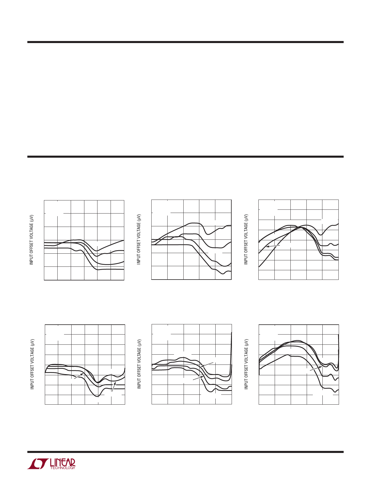
Typical Performance Characteristics
Input Offset Voltage vs Input
Common Mode Voltage
15
VS = 3V
VREF = 0V
10 TA = 25°C
5
0
–5
–10
–15
0
G = 1000
G = 100
G = 10
G=1
0.5 1.0 1.5 2.0 2.5 3.0
INPUT COMMON MODE VOLTAGE (V)
2053 G01
Input Offset Voltage vs Input
Common Mode Voltage
20
VS = 3V
15 VREF = 0V
G = 10
10
5
0
–5
–10
–15
–20
0
TA = 25°C
TA = 85°C
TA = 70°C
TA = –55°C
0.5 1.0 1.5 2.0 2.5 3.0
INPUT COMMON MODE VOLTAGE (V)
2053 G04
Input Offset Voltage vs Input
Common Mode Voltage
15
VS = 5V
VREF = 0V
10 TA = 25°C
G = 1000
5
0
–5
–10
–15
0
G = 100
G=1
G = 10
1
2
3
4
5
INPUT COMMON MODE VOLTAGE (V)
2053 G02
Input Offset Voltage vs Input
Common Mode Voltage
20
VS = 5V
15
VREF = 0V
G = 10
10
5
TA = 85°C
TA = 70°C
0
–5
TA = 25°C
–10
–15
–20
0
TA = –55°C
1
2
3
4
5
INPUT COMMON MODE VOLTAGE (V)
2053 G05
Input Offset Voltage vs Input
Common Mode Voltage
20
VS = ±5V
15
VREF = 0V
TA = 25°C
10
G = 10
G = 1000
5
0
G=1
G = 100
–5
–10
–15
–20
–5
–3
–1
1
3
5
INPUT COMMON MODE VOLTAGE (V)
2053 G03
Input Offset Voltage vs Input
Common Mode Voltage
20
VS = ±5V
15 VREF = 0V
G = 10
10
5
TA = 25°C
TA = 85°C
0
–5
TA = 70°C
–10
–15
TA = –55°C
–20
–5
–3
–1
1
3
5
INPUT COMMON MODE VOLTAGE (V)
2053 G06
2053syncfc
Share Link: