LTC2246LX(RevB) жҹҘзңӢж•ёж“ҡиЎЁпјҲPDFпјү - Linear Technology
йӣ¶д»¶зј–еҸ·
дә§е“ҒжҸҸиҝ° (еҠҹиғҪ)
з”ҹдә§еҺӮ家
LTC2246LX Datasheet PDF : 18 Pages
| |||
LTC2246H
APPLICATIONS INFORMATION
DYNAMIC PERFORMANCE
Signal-to-Noise Plus Distortion Ratio
The signal-to-noise plus distortion ratio [S/(N + D)] is
the ratio between the RMS amplitude of the fundamen-
tal input frequency and the RMS amplitude of all other
frequency components at the ADC output. The output is
band limited to frequencies above DC to below half the
sampling frequency.
is deп¬Ғned as the ratio of the RMS value of either input tone
to the RMS value of the largest 3rd order intermodulation
product.
Spurious Free Dynamic Range (SFDR)
Spurious free dynamic range is the peak harmonic or spuri-
ous noise that is the largest spectral component excluding
the input signal and DC. This value is expressed in decibels
relative to the RMS value of a full scale input signal.
Signal-to-Noise Ratio
The signal-to-noise ratio (SNR) is the ratio between the
RMS amplitude of the fundamental input frequency and
the RMS amplitude of all other frequency components
except the п¬Ғrst п¬Ғve harmonics and DC.
Total Harmonic Distortion
Total harmonic distortion is the ratio of the RMS sum
of all harmonics of the input signal to the fundamental
itself. The out-of-band harmonics alias into the frequency
band between DC and half the sampling frequency. THD
is expressed as:
( ( ) ) THD = 20Log V22 + V32 + V42 + ...Vn2 / V1
where V1 is the RMS amplitude of the fundamental fre-
quency and V2 through Vn are the amplitudes of the second
through nth harmonics. The THD calculated in this data
sheet uses all the harmonics up to the п¬Ғfth.
Intermodulation Distortion
If the ADC input signal consists of more than one spectral
component, the ADC transfer function nonlinearity can
produce intermodulation distortion (IMD) in addition to
THD. IMD is the change in one sinusoidal input caused
by the presence of another sinusoidal input at a different
frequency.
If two pure sine waves of frequencies fa and fb are applied
to the ADC input, nonlinearities in the ADC transfer function
can create distortion products at the sum and difference
frequencies of mfa Вұ nfb, where m and n = 0, 1, 2, 3, etc.
The 3rd order intermodulation products are 2fa + fb, 2fb
+ fa, 2fa вҖ“ fb and 2fb вҖ“ fa. The intermodulation distortion
10
Input Bandwidth
The input bandwidth is that input frequency at which the
amplitude of the reconstructed fundamental is reduced
by 3dB for a full scale input signal.
Aperture Delay Time
The time from when CLK reaches mid-supply to the
instant that the input signal is held by the sample and
hold circuit.
Aperture Delay Jitter
The variation in the aperture delay time from conversion
to conversion. This random variation will result in noise
when sampling an AC input. The signal to noise ratio due
to the jitter alone will be:
SNRJITTER = вҖ“20log (2ПҖ вҖў fIN вҖў tJITTER)
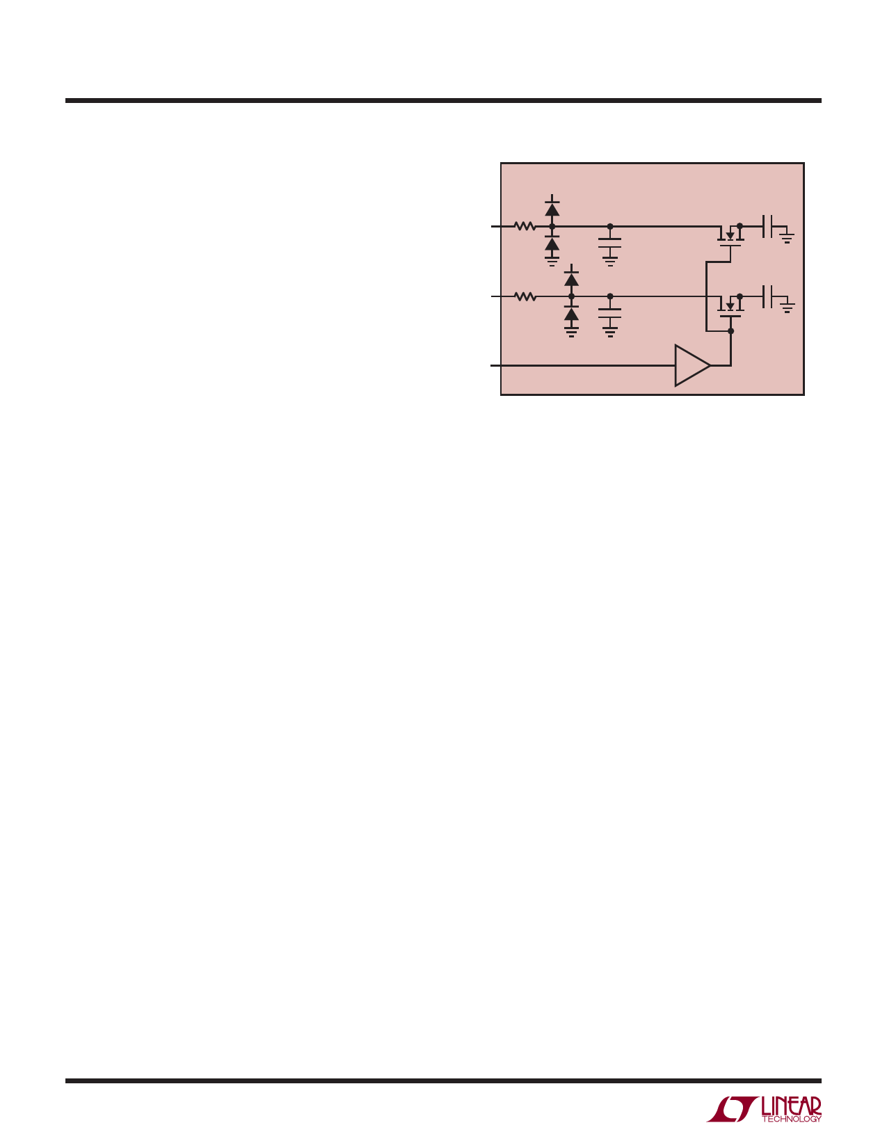
CONVERTER OPERATION
As shown in Figure 1, the LTC2246H is a CMOS pipelined
multistep converter. The converter has six pipelined ADC
stages; a sampled analog input will result in a digitized
value п¬Ғve cycles later (see the Timing Diagram section).
For optimal AC performance the analog inputs should be
driven differentially. For cost sensitive applications, the
analog inputs can be driven single-ended with slightly
worse harmonic distortion. The CLK input is single-ended.
The LTC2246H has two phases of operation, determined
by the state of the CLK input pin.
Each pipelined stage shown in Figure 1 contains an ADC,
a reconstruction DAC and an interstage residue ampliп¬Ғer.
In operation, the ADC quantizes the input to the stage and
the quantized value is subtracted from the input by the
2246hfb
Share Link: 