LTC2931HF 查看數據表(PDF) - Linear Technology
零件编号
产品描述 (功能)
生产厂家
LTC2931HF
Linear Technology

LTC2931HF Datasheet PDF : 16 Pages
| |||
LTC2931
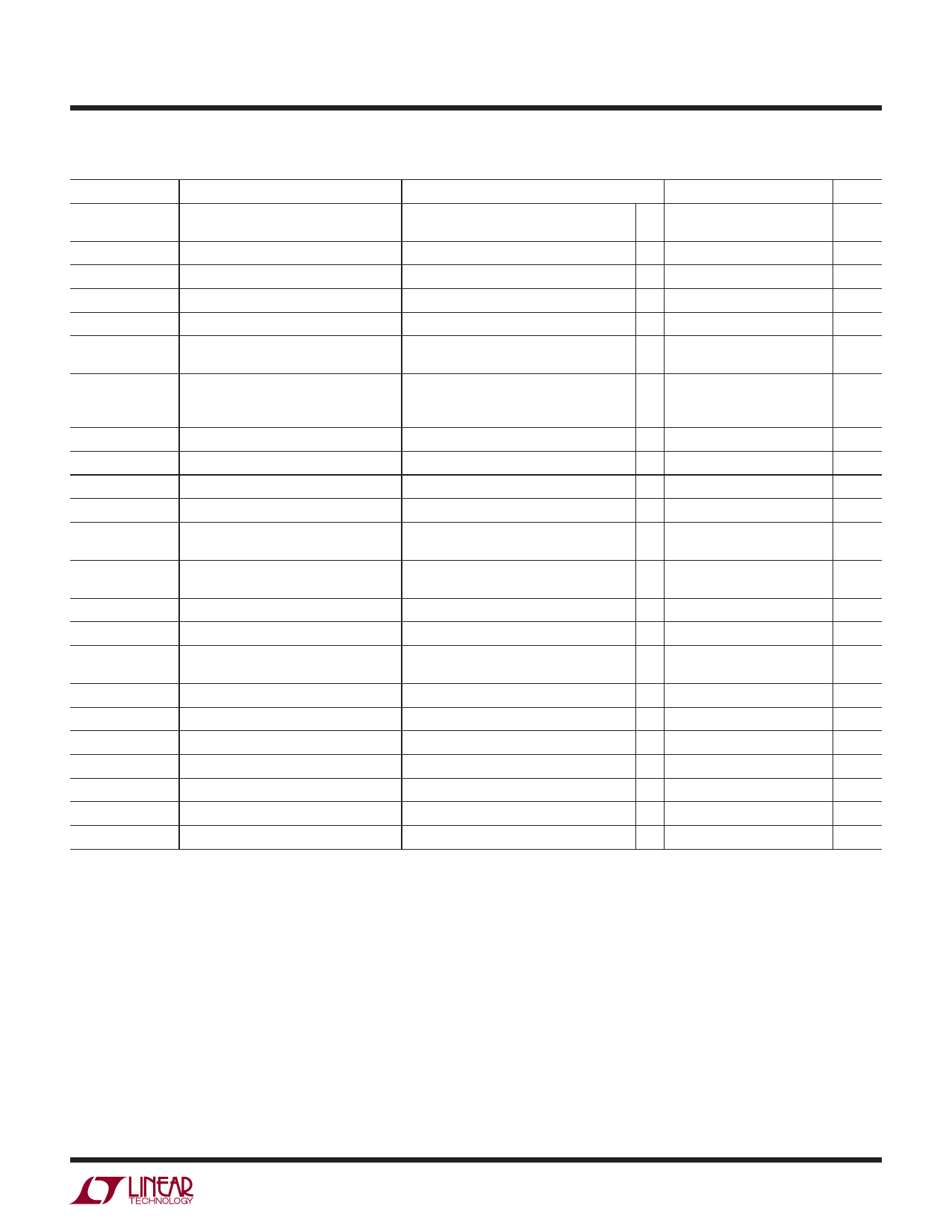
ELECTRICAL CHARACTERISTICS The ● denotes the specifications which apply over the full operating
temperature range, otherwise specifications are at TA = 25°C. VCC = 5V, unless otherwise specified. (Note 3)
SYMBOL
VREF
VPG
IVPG
IV1
IV2
IV3
IV4
IV5, IV6
ICRT(UP)
ICRT(DN)
tRST
tUV
VOL
ICOMPn
VOL
VOH
ICWT(UP)
ICWT(DN)
tWD
VIH
VIL
tWP
IWDI
PARAMETER
CONDITIONS
Reference Voltage
Mode Selection Voltage Range
VPG Input Current
V1 Input Current
V2 Input Current
VCC ≥ 2.3V, IVREF = ±1mA,
CREF ≤ 1000pF
VCC ≥ VCCMINP
VPG = VREF
V1 = 5V, IVREF = 12μA (Note 4)
V2 = 3.3V
V3 Input Current
V3 = 2.5V
V3 = 0.55V (ADJ Mode)
V4 Input Current
V4 = 1.8V
V4 = 0.55V (ADJ Mode)
V4 = –0.02V (–ADJ Mode)
V5, V6 Input Current
V5, V6 = 0.55V
CRT Pull-Up Current
CRT Pull-Down Current
Reset Timeout Period
Vn Undervoltage Detect to RST or
COMPn
Voltage Output Low RST, COMPn
COMPn Pull-Up Current
Voltage Output Low WDO
Voltage Output High RST, WDO, COMPn
(Note 5)
VCRT = GND
VCRT = 1.3V
CRT = 1500pF
Vn Less Than Reset Threshold by More
than 1%
ISINK = 3mA, VCC = 3V
ISINK = 100μA, VCC = 1V
VCOMPn = GND
ISINK = 3mA
ISOURCE = –1μA
CWT Pull-Up Current
CWT Pull-Down Current
Watchdog Timeout Period
WDI Input Threshold High
WDI Input Threshold Low
WDI Input Pulse Width
WDI Pull-Up Current
VCWT = GND
VCWT = 1.3V
CWT = 1500pF
VCC = 3.3V to 5.5V
VCC = 3.3V to 5.5V
VCC = 3.3V
VWDI = 1V
MIN
● 1.192
TYP
1.210
MAX
1.228
UNITS
V
●
0
●
VREF
V
±20
nA
●
52
75
μA
●
0.8
2
μA
●
0.52
1.2
μA
● –15
15
nA
●
0.34
0.8
μA
● –15
15
nA
● –15
15
nA
● –15
15
nA
● –1.4
–2
–2.6
μA
● 10
20
30
μA
●
2
3
4
ms
150
μs
●
0.15
0.4
V
●
0.05
0.3
V
● –2
–6
–12
μA
●
0.15
0.4
V
● V2-1
V
● –1.4
–2
–2.6
μA
● 10
20
30
μA
● 20
30
40
ms
● 1.6
V
●
0.4
V
● 150
ns
● –4
–10
–16
μA
Note 1: Stresses beyond those listed under Absolute Maximum Ratings
may cause permanent damage to the device. Exposure to any Absolute
Maximum Rating condition for extended periods may affect device reliability
and lifetime.
Note 2: All currents into pins are positive, all voltages are referenced to GND
unless otherwise noted.
Note 3: The greater of V1, V2 is the internal supply voltage (VCC).
Note 4: Under static no-fault conditions, V1 will necessarily supply quiescent
current. If at any time V2 is larger than V1, V2 must be capable of supplying
the quiescent current, programming (transient) current and reference load
current.
Note 5: The output pins RST, WDO, and COMPn have diode protected internal
pull-ups to V2 of typically 6μA. However, external pull-up resistors may be used
when faster rise times are required or for VOH voltages greater than V2.
2931fb
3
Share Link: