LTC2932I 查看數據表(PDF) - Linear Technology
零件编号
产品描述 (功能)
生产厂家
LTC2932I
Linear Technology

LTC2932I Datasheet PDF : 16 Pages
| |||
LTC2932
ELECTRICAL CHARACTERISTICS The ● denotes the specifications which apply over the full operating
temperature range, otherwise specifications are at TA = 25°C. VCC = 5V, unless otherwise specified. (Note 3)
SYMBOL
PARAMETER
Digital Inputs T0, T1, RDIS
CONDITIONS
MIN TYP MAX UNITS
VIL
VIH
IINTOL
VIL
VIH
IRDIS
T0, T1 Low Level Input Voltage
T0, T1 High Level Input Voltage
T0, T1 Input Current
RDIS Input Threshold Low
RDIS Input Threshold High
RDIS Pull-Up Current
VCC = 3.3V to 5.5V
VCC = 3.3V to 5.5V
T0, T1 = 2V
VCC = 3.3V to 5.5V
VCC = 3.3V to 5.5V
VRDIS = 1V
●
0.3VCC
V
● 0.7VCC
V
●
±0.1
±1
μA
●
0.4
V
● 1.6
V
● –4
–10
–16
μA
Note 1: Stresses beyond those listed under Absolute Maximum Ratings
may cause permanent damage to the device. Exposure to any Absolute
Maximum Rating condition for extended periods may affect device reliability
and lifetime.
Note 2: All currents into pins are positive, all voltages are referenced to GND
unless otherwise noted.
Note 3: The greater of V1, V2 is the internal supply voltage (VCC).
Note 4: Under static no-fault conditions, V1 will necessarily supply quiescent
current. If at any time V2 is larger than V1, V2 must be capable of supplying
the quiescent current, programming (transient) current and reference load
current.
Note 5: The output pins RST and COMPn have diode protected internal pull-ups
to V2 of typically 6μA. However, external pull-up resistors may be used when
faster rise times are required or for VOH voltages greater than V2.
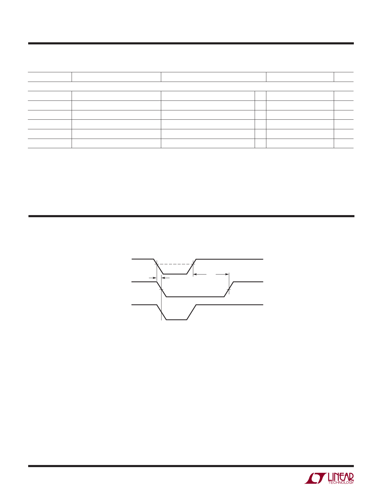
TIMING DIAGRAM
Vn
RST
Vn Monitor Timing
VRT
tUV
tRST
COMPn
2932 TD
2932fb
4
Share Link: