LTC3218EDDB 查看數據表(PDF) - Linear Technology
零件编号
产品描述 (功能)
生产厂家
LTC3218EDDB Datasheet PDF : 12 Pages
| |||
LTC3218
APPLICATIONS INFORMATION
At moderate to high output power, the quiescent current
of the LTC3218 is negligible and the expression above is
valid.
Once dropout is detected at the ILED pin, the LTC3218
enables the charge pump in 2x mode.
In 2x boost mode, the efficiency is similar to that of a
linear regulator with an effective input voltage of 2 times
the actual input voltage. In an ideal 2x charge pump, the
power efficiency would be given by:
ηID E A L
≡
PL E D
PIN
=
VLED • ILED
VIN • 2 • ILED
≈
VL E D
2VIN
Thermal Management
For higher input voltages and maximum output current,
there can be substantial power dissipation in the LTC3218.
If the junction temperature increases above approximately
165°C, the thermal shutdown circuitry will automatically
deactivate the output. To reduce maximum junction tem-
perature, a good thermal connection to the PC board is
recommended. Connecting the Exposed Pad to a ground
plane and maintaining a solid ground plane under the
device can reduce the thermal resistance of the package
and PC board considerably.
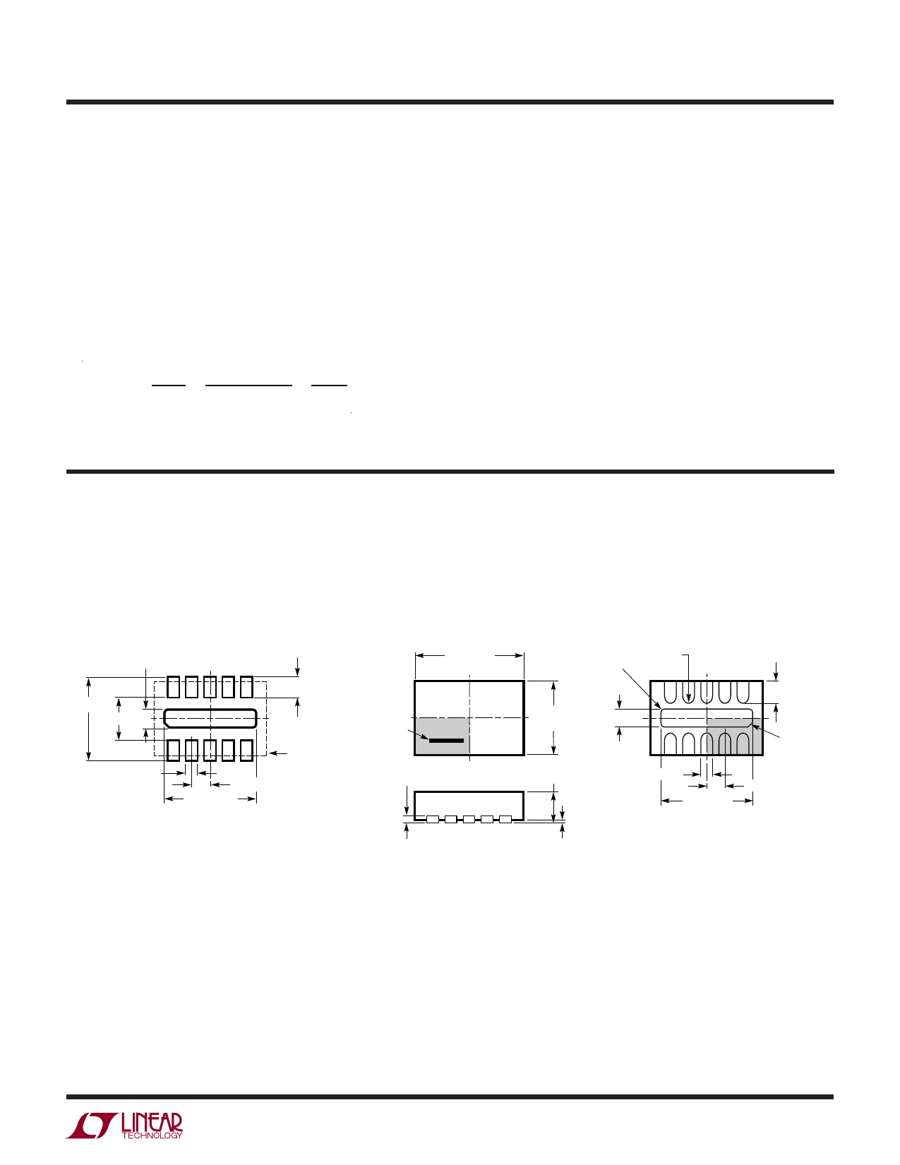
PACKAGE DESCRIPTION
DDB Package
10-Lead Plastic DFN (3mm × 2mm)
(Reference LTC DWG # 05-08-1722 Rev Ø)
0.64 ±0.05
(2 SIDES)
2.55 ±0.05
1.15 ±0.05
0.70 ±0.05
0.25 ± 0.05
0.50 BSC
2.39 ±0.05
(2 SIDES)
PACKAGE
OUTLINE
RECOMMENDED SOLDER PAD PITCH AND DIMENSIONS
PIN 1 BAR
TOP MARK
(SEE NOTE 6)
0.200 REF
3.00 ±0.10
(2 SIDES)
R = 0.05
TYP
R = 0.115
TYP
6
0.40 ± 0.10
10
2.00 ±0.10
(2 SIDES)
0.75 ±0.05
0.64 ± 0.05
(2 SIDES)
5
0.25 ± 0.05
PIN 1
R = 0.20 OR
0.25 × 45°
CHAMFER
1
(DDB10) DFN 0905 REV Ø
0.50 BSC
0 – 0.05
2.39 ±0.05
(2 SIDES)
BOTTOM VIEW—EXPOSED PAD
NOTE:
1. DRAWING CONFORMS TO VERSION (WECD-1) IN JEDEC PACKAGE OUTLINE M0-229
2. DRAWING NOT TO SCALE
3. ALL DIMENSIONS ARE IN MILLIMETERS
4. DIMENSIONS OF EXPOSED PAD ON BOTTOM OF PACKAGE DO NOT INCLUDE
MOLD FLASH. MOLD FLASH, IF PRESENT, SHALL NOT EXCEED 0.15mm ON ANY SIDE
5. EXPOSED PAD SHALL BE SOLDER PLATED
6. SHADED AREA IS ONLY A REFERENCE FOR PIN 1 LOCATION ON THE TOP AND BOTTOM OF PACKAGE
Information furnished by Linear Technology Corporation is believed to be accurate and reliable.
However, no responsibility is assumed for its use. Linear Technology Corporation makes no representa-
tion that the interconnection of its circuits as described herein will not infringe on existing patent rights.
3218fb
11
Share Link: 