LTC3541EDD-3 查看數據表(PDF) - Linear Technology
零件编号
产品描述 (功能)
生产厂家
LTC3541EDD-3 Datasheet PDF : 20 Pages
| |||
LTC3541-3
ABSOLUTE AXI U RATI GS
(Note 1)
Supply Voltages:
VIN, LVIN................................................... –0.3V to 6V
LVIN – VIN...........................................................<0.3V
Pin Voltages:
ENVLDO, ENBUCK, MODE, SW ......–0.3V to VIN + 0.3V
Linear Regulator IOUT(MAX) (100ms) (Note 9).......100mA
Operating Ambient Temperature Range
(Note 2).................................................... –40°C to 85°C
Junction Temperature (Notes 5, 10)...................... 125°C
Storage Temperature Range................... –65°C to 125°C
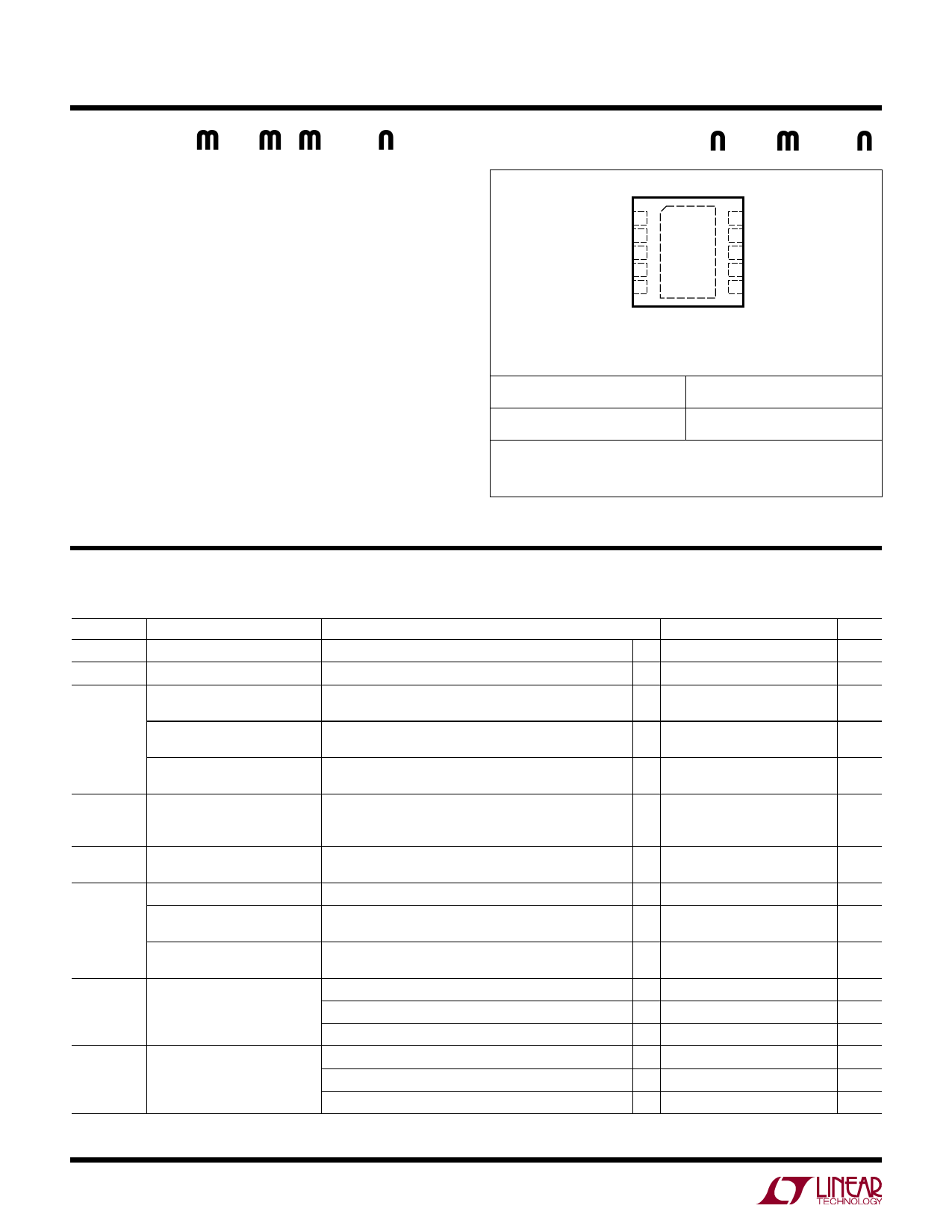
UW U
PACKAGE/ORDER I FOR ATIO
TOP VIEW
VIN 1
ENBUcK 2
VOUT 3
Nc 4
LVOUT 5
10 SW
9 ENVLDO
11
8 MODE
7 GND
6 LVIN
DD PAcKAGE
10-LEAD (3mm × 3mm) PLASTIc DFN
TJMAX = 125°C, θJA = 43°C/W
EXPOSED PAD (PIN 11) IS PGND, MUST BE SOLDERED TO PCB
Order part number DD part marking
LTC3541EDD-3
LCHR
Order Options Tape and Reel: Add #TR
Lead Free: Add #PBF Lead Free Tape and Reel: Add #TRPBF
Lead Free Part Marking: http://www.linear.com/leadfree/
Consult LTC Marketing for parts specified with wider operating temperature ranges.
ELECTRICAL CHARACTERISTICS The ● denotes the specifications which apply over the full operating
temperature range, otherwise specifications are at TA = 25°C. VIN = 3.6V unless otherwise specified (Notes 2, 3).
SYMBOL PARAMETER
CONDITIONS
IPK
Peak Inductor Current
VIN = 4.2V (Note 8)
VIN
Input Voltage Range
(Note 4)
l
VIN(LINEREG) Buck VIN Line Regulation
VIN = 2.7V to 5.5V, ENBUCK = VIN,
l
ENVLDO = 0V, MODE = VIN (Note 6)
VLDO VIN Line Regulation
(Referred to LVOUT)
VIN = 3V to 5.5V, LVOUT = 1.575V, ENBUCK = VIN,
ENVLDO = VIN, MODE = 0V, IOUT(VLDO) = 100mA
Linear Regulator VIN Line
VIN = 3V to 5.5V, LVOUT = 1.575V, ENBUCK = 0V,
Regulation (Referred to LVOUT) ENVLDO = VIN, IOUT(LDO) = 10mA
LVIN(LINEREG) LVIN Line Regulation
(Referred to LVOUT)
VLDODO
LVIN – LVOUT Dropout Voltage
LVIN = 1.675V to 5.5V, VIN = 5.5V, LVOUT = 1.575V,
ENBUCK = VIN, ENVLDO = VIN, MODE = VIN,
IOUT(VLDO) = 100mA
LVOUT = 1.575V, ENBUCK = VIN, ENVLDO = VIN,
MODE = VIN, IOUT(VLDO) = 50mA (Note 9)
VLOADREG Buck Output Load Regulation ENBUCK = VIN, ENVLDO = 0V, MODE = VIN (Note 6)
VVOUT
VLDO Output Load Regulation IOUT(VLDO) = 1mA – 300mA, LVIN = 1.8V, LVOUT = 1.575V, l
ENBUCK = VIN, ENVLDO = VIN, MODE = VIN
Linear Regulator Output Load IOUT(LDO) = 1mA – 30mA, LVOUT = 1.575V,
l
Regulation
ENBUCK = 0V, ENVLDO = VIN
Reference Regulation Voltage ENBUCK = VIN, ENVLDO = 0V, TA = 25°C
(Note 6)
ENBUCK = VIN, ENVLDO = 0V, 0°C ≤ TA ≤ 85°C
ENBUCK = VIN, ENVLDO = 0V, –40°C ≤ TA ≤ 85°C
l
VLVOUT
Reference Regulation Voltage ENBUCK = 0V, ENVLDO = VIN, TA = 25°C
(Note 7)
ENBUCK = 0V, ENVLDO = VIN, 0°C ≤ TA ≤ 85°C
ENBUCK = 0V, ENVLDO = VIN, –40°C ≤ TA ≤ 85°C
l
MIN
0.8
2.7
1.764
1.760
1.755
1.543
1.540
1.536
TYP MAX UNITS
0.95 1.25
A
5.5
V
0.04
0.4
%/V
2.2
mV/V
2.2
mV/V
0.8
mV/V
20
50
mV
0.5
%
0.25
0.5
%
0.25
0.5
%
1.8 1.836
V
1.8 1.840
V
1.8 1.845
V
1.575 1.607
V
1.575 1.610
V
1.575 1.614
V
35413fc
Share Link: 