LTC3541EDD 查看數據表(PDF) - Linear Technology
零件编号
产品描述 (功能)
生产厂家
LTC3541EDD Datasheet PDF : 22 Pages
| |||
LTC3541
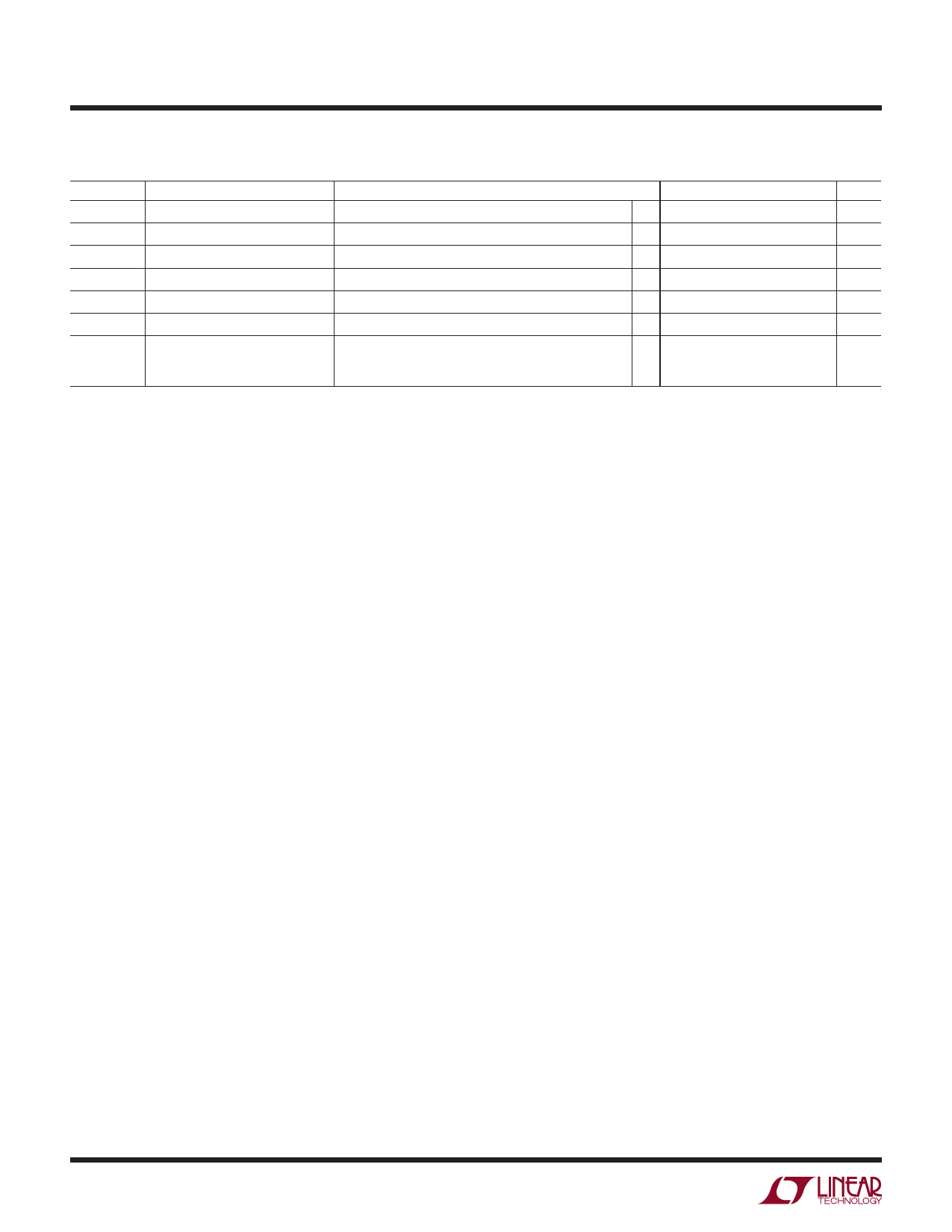
ELECTRICAL CHARACTERISTICS The l denotes the specifications which apply over the full operating
temperature range, otherwise specifications are at TA = 25°C. VIN = 3.6V unless otherwise specified (Note 2)
SYMBOL
fOSC
RPFET
RNFET
ILSW
VIH
VIL
IMODE,
IENBUCK,
IENVLDO
PARAMETER
Oscillator Frequency
RDS(ON) of P-Channel MOSFET
RDS(ON) of N-Channel MOSFET
SW Leakage
Input Pin High Threshold
Input Pin Low Threshold
Input Pin Current
CONDITIONS
ISW = 100mA
ISW = 100mA
Enable = 0V, VSW = 0V or 6V, VIN = 6V
MODE, ENBUCK, ENVLDO
MODE, ENBUCK, ENVLDO
MIN
l 1.8
l 0.9
l
l
TYP
2.25
0.25
0.35
±0.01
±0.01
MAX UNITS
2.7
MHz
Ω
Ω
±1
μA
V
0.3
V
±1
μA
Note 1: Stresses beyond those listed under Absolute Maximum Ratings
may cause permanent damage to the device. Exposure to any Absolute
Maximum Rating condition for extended periods may affect device
reliability and lifetime.
Note 2: The LTC3541 is guaranteed to meet performance specifications
from 0°C to 85°C. VLDO/linear regulator output is tested and specified
under pulse load conditions such that TJ ≈ TA, and are 100% production
tested at 25°C. Specifications over the –40°C to 85°C operating
temperature range are assured by design, characterization and correlation
with statistical process controls.
Note 3: Minimum operating LVIN voltage required for VLDO regulator
regulation is:
LVIN ≥ LVOUT + VDROPOUT and LVIN ≥ 0.9V
Note 4: Minimum operating VIN voltage required for VLDO regulator and
linear regulator regulation is:
VIN ≥ LVOUT + 1.4V and VIN ≥ 2.7V
Note 5: TJ is calculated from the ambient temperature, TA, and power
dissipation, PD, according to the following formula:
TJ = TA + (PD • 43°C/W)
Note 6: The LTC3541 is tested in a proprietary test mode that connects
VBUCKFB to the output of the error amplifier. For the reference regulation
and line regulation tests, the output of the error amplifier is set to the
midpoint. For the load regulation test, the output of the error amplifier is
driven to minimum and maximum of the signal range.
Note 7: Measurement made in closed loop linear regulator configuration
with LVOUT = 1.2V, ILOAD = 10μA.
Note 8: Measurement made in a proprietary test mode with slope
compensation disabled.
Note 9: Measurement is assured by design, characterization and statistical
process control.
Note 10: This IC includes overtemperature protection that is intended
to protect the device during momentary overload conditions. Junction
temperature will exceed 125°C when overtemperature protection is active.
Continuous operation above the specified maximum operating junction
temperature may impair device reliability.
3541fb
4
For more information www.linear.com/LTC3541
Share Link: 