LTC6102HVCDD(RevB) 查看數據表(PDF) - Linear Technology
零件编号
产品描述 (功能)
生产厂家
LTC6102HVCDD Datasheet PDF : 20 Pages
| |||
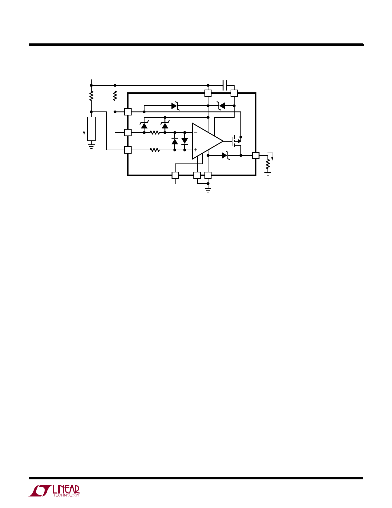
LTC6102/LTC6102HV
APPLICATIONS INFORMATION
must be chosen such that the max output voltage does
not exceed the LTC6102 max output voltage rating. If the
following circuit is a buffer or ADC with limited input range,
then ROUT must be chosen so that IOUT(MAX) • ROUT is less
than the allowed maximum input range of this circuit.
In addition, the output impedance is determined by ROUT. If
the circuit to be driven has high enough input impedance,
then almost any output impedance will be acceptable.
However, if the driven circuit has relatively low input imped-
ance, or draws spikes of current, such as an ADC might
do, then a lower ROUT value may be required in order to
preserve the accuracy of the output. As an example, if the
input impedance of the driven circuit is 100 times ROUT,
then the accuracy of VOUT will be reduced by 1% since:
VOUT
= IOUT
•
ROUT
ROUT
• RIN(DRIVEN)
+ RIN(DRIVEN)
= IOUT
• ROUT
•
100
101
=
0.99
• IOUT
•
ROUT
Error Sources
The current sense system uses an amplifier and resistors
to apply gain and level shift the result. The output is then
dependent on the characteristics of the amplifier, such as
gain and input offset, as well as resistor matching.
Ideally, the circuit output is:
VOUT
=
VSENSE
•
ROUT
RIN
; VSENSE
=
RSENSE
• ISENSE
In this case, the only error is due to resistor mismatch,
which provides an error in gain only.
Output Error, EOUT, Due to the Amplifier DC Offset
Voltage, VOS
EOUT(VOS) = VOS • (ROUT/RIN)
The DC offset voltage of the amplifier adds directly to the
value of the sense voltage, VSENSE. This error is very small
(3μV typ) and may be ignored for reasonable values of RIN.
For very high dynamic range, this offset can be calibrated
in the system due to its extremely low drift.
Output Error, EOUT, Due to the Bias Currents,
IB(+) and IB(–)
The input bias current of the LTC6102 is vanishingly small.
However, for very high resolution, or at high temperatures
where IB increases due to leakage, the current may be
significant.
The bias current IB(+) flows into the positive input of the
internal op amp. IB(–) flows into the negative input.
EOUT(IBIAS) = ROUT((IB(+) • (RSENSE/RIN) – IB(–))
Since IB(+) ≈ IB(–) = IBIAS, if RSENSE << RIN then,
EOUT(IBIAS) ≈ –ROUT • IBIAS
For instance if IBIAS is 1nA and ROUT is 10k, the output
error is –10μV.
Note that in applications where RSENSE ≈ RIN, IB(+) causes
a voltage offset in RSENSE that cancels the error due to
IB(–) and EOUT(IBIAS) ≈ 0. In applications where RSENSE <
RIN, the bias current error can be similarly reduced if an
external resistor RIN(+) = (RIN – RSENSE) is connected as
shown in Figure 4. Under both conditions:
EOUT(IBIAS) = ± ROUT • IOS; IOS = IB(+) – IB(–)
Adding RIN+ as described will maximize the dynamic
range of the circuit. For less sensitive designs, RIN+ is
not necessary.
V+
RIN–
RSENSE
RIN+ +IN
LOAD
V–
+–
–INS
–INF
V+
VREG
0.1μF
LTC6102
RIN+ = RIN– – RSENSE
OUT
VOUT
ROUT
6102 F04
Figure 4. Second Input R Minimizes
Error Due to Input Bias Current
6102fb
11
Share Link: 