5533 查看數據表(PDF) - Linear Technology
零件编号
产品描述 (功能)
生产厂家
5533 Datasheet PDF : 12 Pages
| |||
LTC5533
APPLICATIO S I FOR ATIO
3600
VCC = 3.6V
3200 VOS = 0V
2800
2400
2000
1600
1200
800
TA = –40°C
TA = 25°C
400
TA = 85°C
0
–32 –28 –24 –20 –16 –12 –8 –4 0 4 8 12
RF INPUT POWER (dBm)
5533 F01
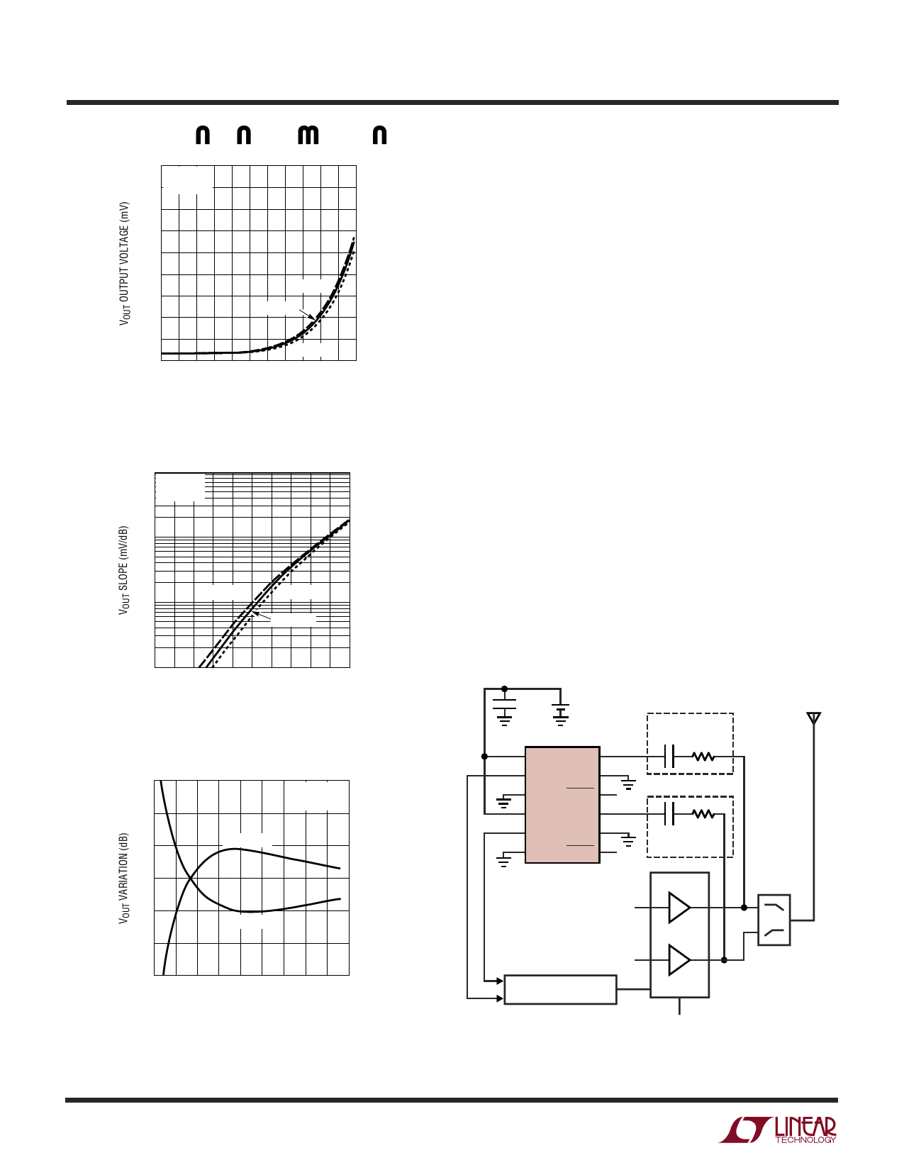
Figure 1. Typical Detector Characteristics, 11GHz
1000
VCC = 3.6V
VOS = 0V
100
TA = –40°C
TA = 85°C
10
TA = 25°C
Figure 2 shows the corresponding slope of the 11GHz
response, and Figure 3 shows the variation of the output
voltage vs RF input power at – 40°C and 85°C, normalized
to the room temperature (25°C) results.
The LTC5533 can be used as a demodulator for AM and
ASK modulated signals with data rates up to 2MHz.
Depending on specific application needs, the detector
outputs can be split between two branches, providing AC-
coupled data (or audio) output and a DC-coupled RSSI
output for signal strength measurements and AGC.
The LTC5533 can also be used for RF power detection and
control. Figure 4 is an example of an LTC5533 used for
dual band mobile phone transmitter power control.
The LTC5533 consists of two separate RF detector dice
packaged together. Consequently, detector-to-detector
isolation is good—typically 45dB at 2GHz. Output match-
ing is good, but not precise. The characterization plots in
the Typical Performance Characteristics show that the
typical output voltage mismatch is within ±25mV with no
RF input signal present. With –14dBm RF input signal, the
typical equivalent mismatch is within ±1dB.
1
–32 –28 –24 –20 –16 –12 –8 –4 0 4 8
RF INPUT POWER (dBm)
5533 F02
Figure 2. VOUT Slope vs RF Input Power at 11GHz
3
VCC = 3.6V
VOS = 0V
2
1
TA = –40°C
0
–1
TA = 85°C
–2
–3
–24 –20 –16 –12 –8 –4 0 4
RF INPUT POWER (dBm)
8 12
5533 F03
Figure 3. VOUT Variation at –40°C and at 85°C vs RF Input Power
at 11GHz, Normalized to Room Temperature (25°C) Results.
10
C3 +
0.1µF
Li-Ion
LTC5533
1
VCC1
2
VOUT1
3
VOS1
4
VCC2
5
VOUT2
6
VOS2
12
RFIN1
11
GND
10
SHDN1
9
RFIN2
8
GND
7
SHDN2
20dB RESISTIVE TAP
C1
39pF R1
360Ω
ANTENNA
14dB RESISTIVE TAP
C2
39pF
R2
150Ω
CELL BAND
DIPLEXER
PCS BAND
MOBILE PHONE BB/DSP
VPC
BSE
5533 F04
Tx PA MODULE
Figure 4. Dual Band Mobile Phone Transmitter
Power Contol with LTC5533
5533f
Share Link: 