5533 查看數據表(PDF) - Linear Technology
零件编号
产品描述 (功能)
生产厂家
5533 Datasheet PDF : 12 Pages
| |||
LTC5533
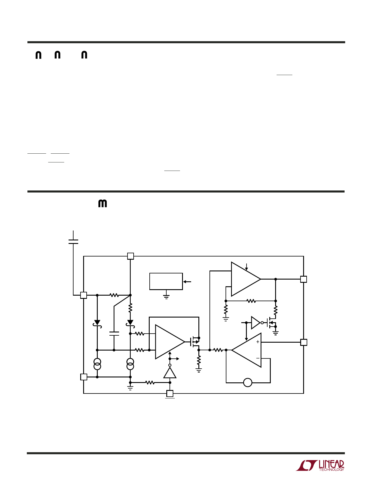
PI FU CTIO S
VCC1, VCC2 (Pins 1, 4): Power Supply Voltage, 2.7V to 6V.
VCC should be bypassed appropriately with ceramic
capacitors.
VOUT1, VOUT2 (Pins 2, 5): Detector Outputs.
VOS1, VOS2 (Pins 3, 6): VOUT Offset Voltage Adjustments.
These pins adjust the starting VOUT voltage when no RF
signal is present. For VOS from 0V to 130mV, VOUT is
unaffected by VOS. For VOS > 130mV, VOUT is the sum of
VOS plus the detected RF signal.
SHDN1, SHDN2 (Pin 10, 7): Shutdown Inputs. A logic low
on the SHDN pin places the corresponding detector in
shutdown mode. A logic high enables the detector. SHDN
has an internal 160k pulldown resistor to ensure that the
detector is shutdown when no SHDN input is applied. In
shutdown VOUT is connected to ground via a 280Ω resis-
tor. Channels can be shut down independently.
GND1, GND2 (Pins 11, 8): Ground.
RFIN1, RFIN2 (Pins 12, 9): RF Input Voltage. Referenced
to VCC. A coupling capacitor must be used to connect to
the RF signal source. These pins have internal 500Ω
terminations, Schottky diode detectors and peak detector
capacitors.
Exposed Pad (Pin13): Ground.
BLOCK DIAGRA (One Channel)
RFSOURCE
12pF TO 200pF
(DEPENDING ON
APPLICATION)
VCC
ONE CHANNEL
BIAS
SD
500Ω
RFIN
500Ω
SD
+
BUFFER
–
30k
30k
31k
25pF
24k
50µA
50µA
+
RF DET
–
SD
SD
80k
80k
GND
160k
120mV+
SHDN
VOUT
180Ω
100Ω
VOS
5531 BD
5533f
8
Share Link: 