LTC6915IDE 查看數據表(PDF) - Linear Technology
零件编号
产品描述 (功能)
生产厂家
LTC6915IDE
Linear Technology

LTC6915IDE Datasheet PDF : 18 Pages
| |||
LTC6915
Operation
1
LTC6915
SHDN #1
V+ 16
0.1µF 2
IN–
15
OUT
3
VIN
IN+
14
SENSE
–5V
4
V–
13
REF
0.1µF
5
12
HOLD_THRU NC
CS
6
11
CS(D0)
P/S
µP DIN
CLK
7
DIN(D1)
10
DGND
8
9
CLK(D2) DOUT(D3)
0.1µF
VOUT
–5V
0.1µF
–5V
LTC6915
1
SHDN
#2
V+ 16
0.1µF 2 IN–
15
OUT
VIN 3 IN+
14
SENSE
4 V–
13
REF
5
12
HOLD_THRU NC
6
CS(D0)
11
P/S
7
DIN(D1)
10
DGND
8
9
CLK(D2) DOUT(D3)
VOUT
0.1µF
–5V
DOUT
CLK
DIN
D15
D11
D10
D9
D8
D7
D3
D2
D1
D0
CS/LD
GAIN CODE FOR #2
GAIN CODE FOR #1
6915 F04
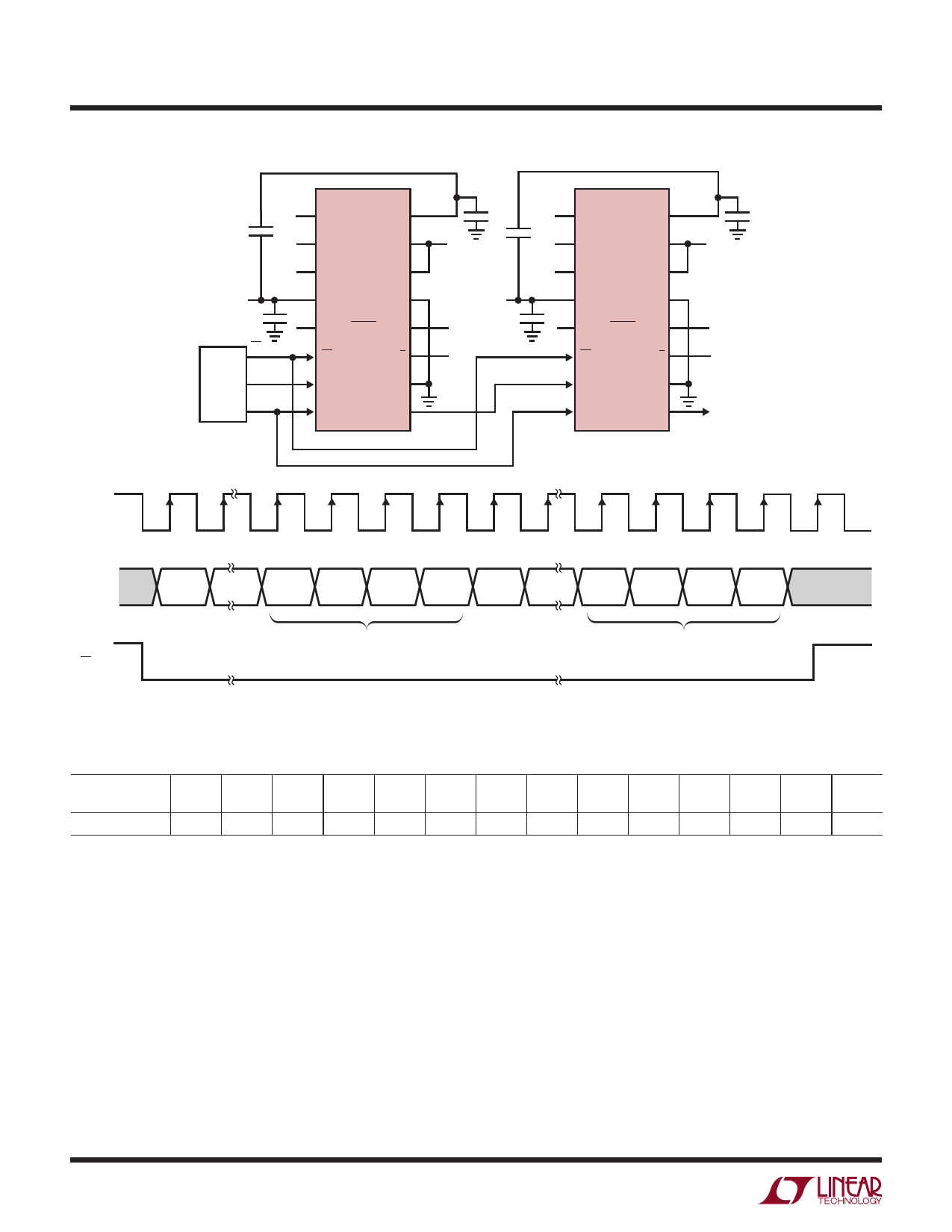
Figure 4. 2 PGAs in a Daisy Chain
The amplifier’s gain is set as follows:
D3, D2, D1, D0
Gain
0000 0001 0010 0011 0100 0101 0110 0111 1000 1001 1010 1011 1100 1101~
1111
0
1
2
4
8
16
32
64 128 256 512 1024 2048 4096
Input Voltage Range
The input common mode voltage range of the LTC6915
is rail-to-rail. However, the following equation limits the
size of the differential input voltage:
V– ≤ (VIN+ – VIN–) + VREF ≤ V+ – 1.3
Where VIN+ and VIN– are the voltage of the differential
input pins, V+ and V– are the positive and negative sup-
ply voltages respectively and VREF is the voltage of REF
pin. In addition, VIN+ and VIN– must not exceed the power
supply voltages, i.e.,
V– < VIN+ < V+ and V– < VIN– < V+
14
±5 Volt Operation
When using the LTC6915 with supplies over 5.5V, care must
be taken to limit the maximum difference between any of
the input pins (IN+ or IN– ) and the REF pin to 5.5V, i.e.,
|VIN+ – VREF| < 5.5 and |VIN– – VREF| < 5.5
If not, the device will be damaged. For example, if rail-
to-rail input operation is desired when the supplies are at
±5V, the REF pin should be 0, ±0.5V. As a second example,
if the V+ pin is 10V, and the V– and REF pins are at 0, the
inputs should not exceed 5.5V.
6915fb
Share Link: