TC2054 查看數據表(PDF) - Microchip Technology
零件编号
产品描述 (功能)
生产厂家
TC2054 Datasheet PDF : 22 Pages
| |||
TC2054/2055/2186
1.0 ELECTRICAL
CHARACTERISTICS
Absolute Maximum Ratings †
Input Voltage ......................................................... 6.5V
Output Voltage ............................... (-0.3) to (VIN + 0.3)
Operating Temperature .................. -40°C < TJ< 125°C
Storage Temperature ......................... -65°C to +150°C
Maximum Voltage on Any Pin ........ VIN +0.3V to -0.3V
† Notice: Stresses above those listed under “Absolute
Maximum Ratings” may cause permanent damage to
the device. These are stress ratings only and functional
operation of the device at these or any other conditions
above those indicated in the operation sections of the
specifications is not implied. Exposure to Absolute
Maximum Rating conditions for extended periods my
affect device reliability.
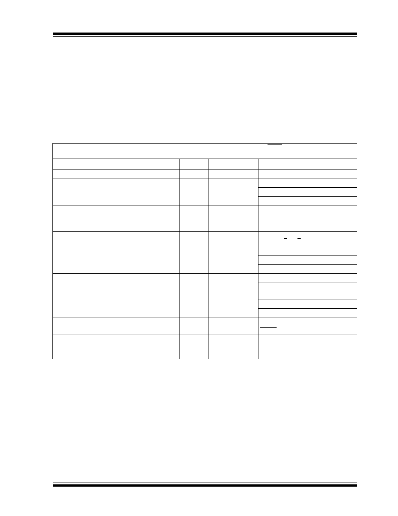
ELECTRICAL SPECIFICATIONS
Electrical Specifications: Unless otherwise noted, VIN = VR + 1V, IL = 100 µA, CL = 3.3 µF, SHDN > VIH, TA = +25°C.
BOLDFACE type specifications apply for junction temperature of -40°C to +125°C.
Parameter
Sym
Min
Typ
Max Units
Conditions
Input Operating Voltage
VIN
2.7
—
Maximum Output Current
IOUTMAX
50
—
100
—
6.0
V Note 1
—
mA TC2054
—
TC2055
150
—
—
TC2186
Output Voltage
VOUT Temperature
Coefficient
VOUT
TCVOUT
VR - 2.0% VR ± 0.4% VR + 2.0% V Note 2
—
20
—
ppm/°C Note 3
—
40
—
Line Regulation
Load Regulation
ΔVOUT/
—
ΔVIN
ΔVOUT/
-1.0
VOUT
-2.0
0.05
0.33
0.43
0.5
+1.0
+2.0
% (VR + 1V) < VIN < 6V
% TC2054;TC2055 IL = 0.1 mA to IOUTMAX
TC2186
IL = 0.1 mA to IOUTMAX
Note 6
Dropout Voltage, Note 7
VIN – VOUT
—
—
—
—
2
—
mV
IL = 100 µA
45
70
IL = 50 mA
90
140
TC2015; TC2185 IL = 100 mA
140
210
TC2185
IL = 150 mA
Note 7
Supply Current
IIN
—
Shutdown Supply Current
IINSD
—
Power Supply Rejection
PSRR
—
Ratio
55
0.05
50
80
µA SHDN = VIH, IL=0
0.5
µA SHDN = 0V
—
dB FRE ≤ 100 kHz
Output Short Circuit Current IOUTSC
160
300
—
mA VOUT = 0V
Note 1:
2:
3:
4:
5:
The minimum VIN has to meet two conditions: VIN = 2.7V and VIN = VR + VDROPOUT.
VR is the regulator output voltage setting. For example: VR = 1.8V, 2.7V, 2.8V, 2.85V, 3.0V, 3.3V.
TCVOUT =
(---V----O-----U-----T----M------A----X------–----V----O------U----T----M------I--N-----)---×-----1----0---6--
VOUT × ΔT
6: Regulation is measured at a constant junction temperature using low duty cycle pulse testing. Load regulation is tested
over a load range from 1.0 mA to the maximum specified output current. Changes in output voltage due to heating
effects are covered by the thermal regulation specification.
7: Dropout voltage is defined as the input to output differential at which the output voltage drops 2% below its nominal
value at a 1V differential.
8: Thermal Regulation is defined as the change in output voltage at a time T after a change in power dissipation is applied,
excluding load or line regulation effects. Specifications are for a current pulse equal to IMAX at VIN = 6V for T = 10 ms.
9: The maximum allowable power dissipation is a function of ambient temperature, the maximum allowable junction tem-
perature and the thermal resistance from junction-to-air (i.e. TA, TJ, θJA).
10: Hysteresis voltage is referenced by VR.
11: Time required for VOUT to reach 95% of VR (output voltage setting), after VSHDN is switched from 0 to VIN.
© 2009 Microchip Technology Inc.
DS21663D-page 3
Share Link: 