LV4901H وں¥çœ‹و•¸و“ڑè،¨ï¼ˆPDF) - SANYO -> Panasonic
零ن»¶ç¼–هڈ·
ن؛§ه“پوڈڈè؟° (هٹں能)
ç”ںن؛§هژ‚ه®¶
LV4901H
SANYO -> Panasonic

LV4901H Datasheet PDF : 14 Pages
| |||
LV4901H
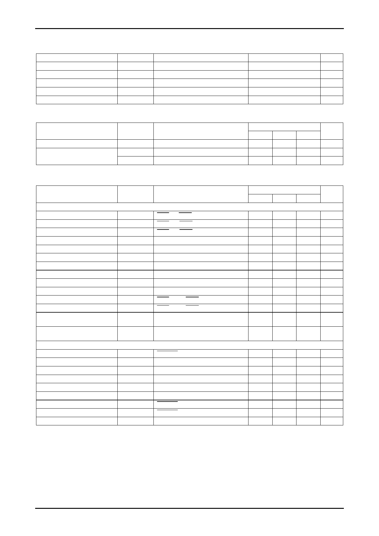
Specifications
Absolute Maximum Ratings at Ta = 25آ°C
Parameter
Maximum supply voltage
Maximum output current
Allowable power dissipation
Operating temperature
Storage temperature
Symbol
VD
IO peak
Pd max
Topr
Tstg
Conditions
Externally applied voltage
Independent package
Recommended Operating Conditions at Ta = 25آ°C
Parameter
Recommended supply voltage range
Recommended load resistance
Symbol
VD
RL (SP)
RL (HP)
Conditions
Externally applied voltage
Speaker load
Headphone
Ratings
14
3.5
886
-25 to +75
-50 to +150
Unit
V
A/ch
mW
آ°C
آ°C
Ratings
Unit
min
typ
max
10
12
13.5
V
4
8
خ©
16
خ©
Electrical Characteristics at Ta = 25آ°C
Parameter
Symbol
Conditions
Ratings
Unit
min
typ
max
Digital amplifier block : VD = 12V, RL = 8خ©, L = 22خ¼H, C = 0.33خ¼F, CL = 1خ¼F
Standby current
Ist
STBY = L, MUTE = L
13
25
خ¼A
Mute current
Imute
STBY = H, MUTE = L
13
20
mA
Quiescent current
Voltage gain
Output offset voltage
ICCO
VG
Voffset
STBY = H, MUTE = H
fin = 1kHz, VO = 0dBm
Rg = 0
27
-150
60
70
mA
29
31
dB
150
mV
Total harmonic distortion
Maximum output
Channel separation
Ripple rejection ratio
THD@1W
PO1@10%
CH sep.
SVRR
PO = 1W, fin = 1kHz, AES17
THD+N = 10%, AES17
fin = 1kHz, VO = 0dBm, Rg = 0, DIN AUDIO
fr = 100Hz, Vr = 0dBm, Rg = 0, A-weight
0.2
0.8
%
8
10
W
55
70
dB
35
50
dB
Noise
VNO
Rg = 0, A-weight
High-level input voltage
VIH
STBY pin and MUTE pin
Low-level input voltage
VIL
STBY pin and MUTE pin
Power supply voltage drop protection UV_UPPER VD pin voltage monitor
circuit upper limit value
Power supply voltage drop protection UV_LOWER VD pin voltage monitor
circuit lower limit value
Headphone amplifier block : VD = 12V, RL = 16خ©, fin = 1kHz
Quiescent current
ICCOhp
HP_STBY = H
Voltage gain
VG
VO = -10dBm
Total harmonic distortion
THD
PO = 1mW, DIN AUDIO
Maximum output
PO
THD = 10%, DIN AUDIO
Channel separation
CH sep.
fin = 1kHz, Vr = 0dBm, Rg = 0, DIN AUDIO
200
500 خ¼Vrms
3
V
1
V
8.0
V
7.0
V
5.5
10
12
0.25
60
80
35
45
9.5
mA
14
dB
0.8
%
mW
dB
Ripple rejection ratio
SVRR
fr = 100Hz, Vr = 0dBm, Rg = 0, DIN AUDIO
55
70
dB
High-level input voltage
VIH
HP_STBY pin
3
V
Low-level input voltage
VIL
HP_STBY pin
1
V
Noise
VNO
Rg = 0خ©, DIN AUDIO
50
200 خ¼Vrms
Note : The values of these characteristics were measured in the SANYO test environment. The actual values in an end system will vary depending on the
printed circuit board pattern, the external components actually used, and other factors.
No.A0098-2/14
Share Link: