LV4985VH وں¥çœ‹و•¸و“ڑè،¨ï¼ˆPDF) - SANYO -> Panasonic
零ن»¶ç¼–هڈ·
ن؛§ه“پوڈڈè؟° (هٹں能)
ç”ںن؛§هژ‚ه®¶
LV4985VH Datasheet PDF : 15 Pages
| |||
LV4985VH
Continued from preceding page.
Pin No.
Pin Name
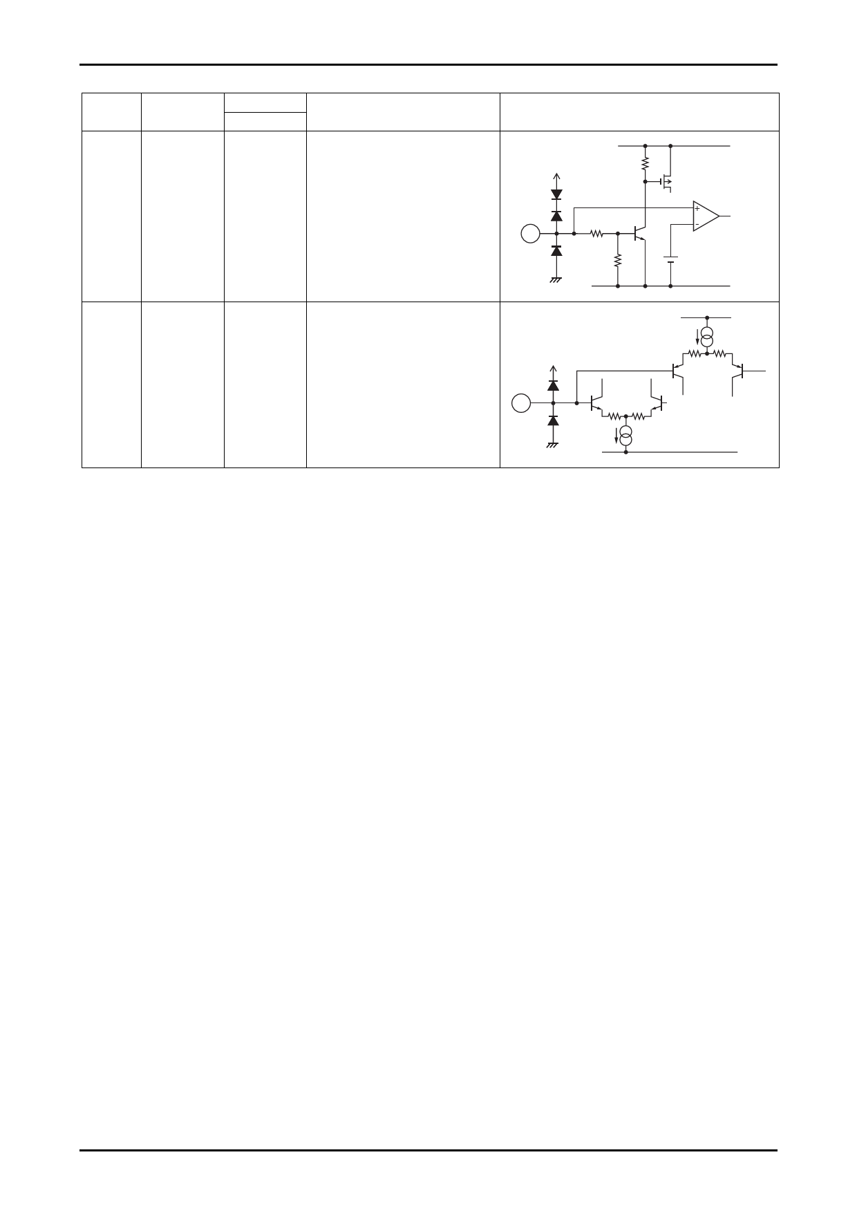
9
STBY
Pin Voltage
VCC = 5V
External apply
Description
Standby/2nd amplifier stop control pin.
0 to 0.3V ⇒ Standby mode
1.3 to 1.7V ⇒ SE mode
2.3 to VCC ⇒ BTL mode
10
VOL
External apply Volume control pin.
Equivalent Circuit
VCC
VCC
30kخ©
9
150kخ©
VCC
VB1
GND
VCC
10
GND
Usage Note
1. Input coupling capacitor (C1 and C2)
C1 (C2) is an input coupling capacitor that is used to cut the DC component. The input coupling capacitor C1 (C2) and
the input resisters of 20kخ© (15kخ© + 5kخ©) make up a high-pass filter, attenuating the bass frequency. Therefore, the
capacitance value must be selected with due consideration of the cut-off frequency.
The cut-off frequencies are expressed by the following formulas.
1ch ⇒ fc1 = 1/ (2د€ أ— C1 أ— 20000)
2ch ⇒ fc2 = 1/ (2د€ أ— C2 أ— 20000)
This capacitor affects the pop noise at startup. Note with care that increasing the capacitance value lengthens the
charging time of the capacitor, which will make the pop noise louder.
2. Input coupling capacitors (C3 and C4) in the power amplifier block
C3 (C4) is an input coupling capacitor that is used to cut the DC component. The input coupling capacitor C3 (C4) and
the input resistor R1 (R3) make up a high-pass filter, attenuating the bass frequency. Therefore, the capacitance value
must be selected with due consideration of the cut-off frequency.
The cut-off frequencies are expressed by the following formulas.
1ch ⇒ fc3 = 1/ (2د€ أ— C3 أ— R1)
2ch ⇒ fc4 = 1/ (2د€ أ— C4 أ— R3)
This capacitor affects the pop noise at startup. Note with care that increasing the capacitance value lengthens the
charging time of the capacitor, which will make the pop noise louder.
3. BTL voltage gain of the power amplifier block
The voltage gain of the first amplifier is determined by the ratio between the resistors R1 and R2 (R3 and R4).
1ch ⇒ Vg1 = 20 أ— log (R2/R1) … unit : dB
2ch ⇒ Vg2 = 20 أ— log (R4/R3) … unit : dB
Therefore, the BTL voltage gain of the power amplifier block is expressed by the following formulas.
1ch ⇒ VgBTL1 = 6 + 20 أ— log (R2/R1) … unit : dB
2ch ⇒ VgBTL2 = 6 + 20 أ— log (R4/R3) … unit : dB
The BTL voltage gain of the power amplifier block must be set in the range of 0 to 26dB.
No.A1568-8/15
Share Link: 