LV8732V 查看數據表(PDF) - SANYO -> Panasonic
零件编号
产品描述 (功能)
生产厂家
LV8732V Datasheet PDF : 26 Pages
| |||
LV8732V
Continued from preceding page.
Parameter
Symbol
Conditions
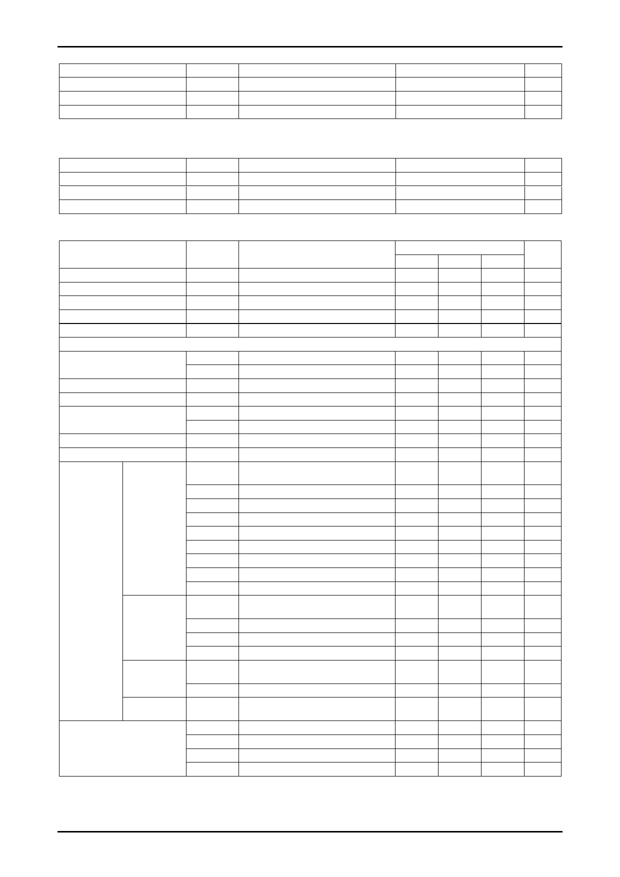
Allowable power dissipation
Pd max
Ta ≤ 85°C *
Operating temperature
Topr
Storage temperature
Tstg
* Specified circuit board : 90.0mm×90.0mm×1.6mm, glass epoxy 2-layer board, with backside mounting.
Allowable Operating Ratings at Ta = 25°C
Parameter
Symbol
Supply voltage range
VM
Logic input voltage
VREF input voltage range
VIN
VREF
Conditions
Ratings
Unit
3.25
W
-20 to +85
°C
-55 to +150
°C
Ratings
Unit
9 to 32
V
0 to 5.5
V
0 to 3
V
Electrical Characteristics at Ta = 25°C, VM = 24V, VREF = 1.5V
Parameter
Symbol
Conditions
Standby mode current drain
Current drain
VREG5 output voltage
Thermal shutdown temperature
Thermal hysteresis width
Motor driver
Output on resistance
Output leakage current
Diode forward voltage
Logic pin input current
Logic high-level input voltage
Logic low-level input voltage
Current setting
comparator
threshold
voltage
(current step
switching)
2W1-2-phase
drive
W1-2-phase
drive
1-2 phase drive
IMst
IM
Vreg5
TSD
ΔTSD
Ronu
Rond
IOleak
VD
IINL
IINH
VINH
VINL
Vtdac0_2W
Vtdac1_2W
Vtdac2_2W
Vtdac3_2W
Vtdac4_2W
Vtdac5_2W
Vtdac6_2W
Vtdac7_2W
Vtdac8_4W
Vtdac0_W
Vtdac2_W
Vtdac4_W
Vtdac6_W
Vtdac0_H
2 phase drive
Vtdac4_H
Vtdac4_F
Current setting comparator
threshold voltage
(current attenuation rate switching)
Vtatt00
Vtatt01
Vtatt10
Vtatt11
ST = “L”
ST = “H”, OE = “L”, with no load
IO = -1mA
Design guarantee
Design guarantee
IO = 2A, Upper-side on resistance
IO = 2A, Lower-side on resistance
ID = -2A
VIN = 0.8V
VIN = 5V
Step 0 (When initialized : channel 1
comparator level)
Step 1 (Initial state+1)
Step 2 (Initial state+2)
Step 3 (Initial state+3)
Step 4 (Initial state+4)
Step 5 (Initial state+5)
Step 6 (Initial state+6)
Step 7 (Initial state+7)
Step 8 (Initial state+8)
Step 0 (When initialized : channel 1
comparator level)
Step 2 (Initial state+1)
Step 4 (Initial state+2)
Step 6 (Initial state+3)
Step 0 (When initialized : channel 1
comparator level)
Step 4 (Initial state+1)
Step 4' (When initialized : channel 1
comparator level)
ATT1 = L, ATT2 = L
ATT1 = H, ATT2 = L
ATT1 = L, ATT2 = H
ATT1 = H, ATT2 = H
min
4.5
150
Ratings
typ
100
3.2
5
180
40
Unit
max
400
μA
5
mA
5.5
V
200
°C
°C
4
30
2.0
0.291
0.285
0.267
0.240
0.201
0.157
0.107
0.053
0.201
0.291
0.267
0.201
0.107
0.291
0.201
0.291
0.291
0.232
0.143
0.053
0.3
0.4
Ω
0.25
0.33
Ω
50
μA
1.2
1.4
V
8
12
μA
50
70
μA
V
0.8
V
0.3
0.309
V
0.294
0.276
0.249
0.21
0.165
0.114
0.06
0.21
0.3
0.303
V
0.285
V
0.258
V
0.219
V
0.173
V
0.121
V
0.067
V
0.219
V
0.309
V
0.276
0.21
0.114
0.3
0.285
V
0.219
V
0.121
V
0.309
V
0.21
0.219
V
0.3
0.309
V
0.3
0.309
V
0.24
0.248
V
0.15
0.157
V
0.06
0.067
V
Continued on next page.
No.A1483-2/26
Share Link: 