LX1669 查看數據表(PDF) - Microsemi Corporation
零件编号
产品描述 (功能)
生产厂家
LX1669 Datasheet PDF : 14 Pages
| |||
PRODUCT DATABOOK 1996/1997
LX1669
PROGRAMMABLE DC:DC CONTROLLER
PRODUCTION DATA SHEET
A B S O L U T E M A X I M U M R AT I N G S (Note 1 & 2)
12V Supply Voltage (VCC12) .................................................................................. 18V
5V Supply Voltage (VCC5) ....................................................................................... 7V
Output Drive Peak Current Source (500ns) ....................................................... 1.0A
Output Drive Peak Current Sink (500ns) ........................................................... 1.0A
Input Voltage (SS, VID[0:4]) ................................................................... -0.3V to 6V
Operating Junction Temperature .................................................................... 150°C
Storage Temperature Range ........................................................... -65°C to +150°C
Lead Temperature (Soldering, 10 Seconds) .................................................... 300°C
Note 1. Exceeding these ratings could cause damage to the device. All voltages are with
respect to Ground. Currents are positive into, negative out of the specified
terminal.
Note 2. VCC3 supply is used as input to internal low dropout regulator. Voltages above
3.3V will cause increased thermal dissipation in the package. Power dissipation
should be limited to keep junction temperature below maximum rating.
T H E R MAL DATA
D PACKAGE:
THERMAL RESISTANCE-JUNCTION TO AMBIENT, θJA
120°C/W
Junction Temperature Calculation: TJ = TA + (PD x θJA).
The θJA numbers are guidelines for the thermal performance of the device/pc-board
system. All of the above assume no ambient airflow.
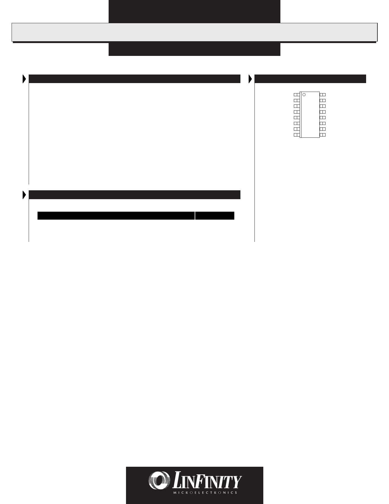
PACKAGE PIN OUTS
TDRV
VCC12
VCC5
PWRGD
OVP
VID0
VID1
VID2
1 16
2
15
3
14
4
13
5
12
6
11
7
10
8
9
PGND
BDRV
AGND
SS/ENABLE
VFB
VCORE
VID4
VID3
D PACKAGE
(Top View)
2
Copyright © 1999
Rev. 1.0 4/99
Share Link: 