M24164-BN3 查看數據表(PDF) - STMicroelectronics
零件编号
产品描述 (功能)
生产厂家
M24164-BN3 Datasheet PDF : 16 Pages
| |||
M24164
Table 2. Absolute Maximum Ratings (1)
Symbol
TA
TSTG
TLEAD
Parameter
Ambient OperatingTemperature(2)
Storage Temperature
Lead Temperature, Soldering
(PSDIP8 package)
(SO8 package)
10 sec
40 sec
Value
Unit
–40 to 125
°C
–65 to 150
°C
260
215
°C
VIO
Input or Output Voltages
–0.6 to 6.5
V
VCC
VESD
Supply Voltage
Electrostatic Discharge Voltage (Human Body model) (3)
Electrostatic Discharge Voltage (Machine model) (4)
–0.3 to 6.5
V
4000
V
500
V
Notes: 1. Except for the rating "Operating Temperature Range", stresses above those listed in the Table "Absolute Maximum Ratings"
may cause permanent damage to the device. These are stress ratings only and operation of the device at these or any other
conditions above those indicated in the Operating sections of this specification is not implied. Exposure to Absolute Maximum
Rating conditions for extended periods may affect device reliability. Refer also to the STMicroelectronics SURE Program and other
relevant quality documents.
2. Depends on range.
3. MIL-STD-883C, 3015.7 (100pF, 1500 Ω).
4. EIAJ IC-121 (Condition C) (200pF, 0 Ω).
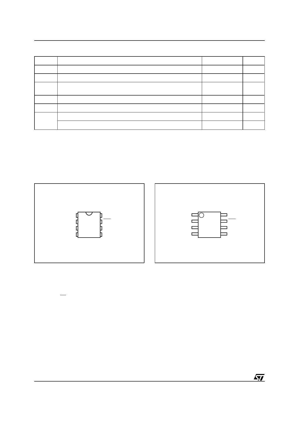
Figure 2A. DIP Pin Connections
Figure 2B. SO Pin Connections
M24164
E0 1
E1 2
E2 3
VSS 4
8 VCC
7 WC
6 SCL
5 SDA
AI02265
E0
E1
E2
VSS
M24164
1
8
2
7
3
6
4
5
AI02266
VCC
WC
SCL
SDA
DESCRIPTION (cont’d)
The memory is compatible with the two wire serial
interface which uses a bi-directional data bus and
serial clock. The memory offers 3 chip enable
inputs (E2, E1, E0) so that up to 8 x 16K devices
may be attached to the bus and selected individu-
ally. The memory behaves as a slave device with
all memory operations synchronized by the serial
clock.
Read and write operations are initiated by a START
condition generated by the bus master. The START
condition is followed by a stream of 7 bits, plus one
read/write bit and terminated by an acknowledge
bit (see Table 3). When writing data to the memory
it responds to the 8 bits received by asserting an
acknowledge bit during the 9th bit time. When data
is read by the bus master, it acknowledges the
receipt of the data bytes in the same way. Data
transfers are terminated with a STOP condition.
Power On Reset: VCC lock out write protect. In
order to prevent any possible data corruption and
inadvertent write operations during power up, a
Power On Reset (POR) circuit is implemented.
Until the VCC voltage has reached the POR thresh-
old value, the internal reset is active, all operations
are disabled and the device will not respond to any
command. In the same way, when VCC drops down
from the operating voltage to below the POR
threshold value, all operations are disabled and the
device will not respond to any command. A stable
VCC must be applied before applying any logic
signal.
2/16
Share Link: 