M24164-BN3 查看數據表(PDF) - STMicroelectronics
零件编号
产品描述 (功能)
生产厂家
M24164-BN3 Datasheet PDF : 16 Pages
| |||
M24164
Acknowledge Bit (ACK). An acknowledge signal
is used to indicate a successful data transfer. The
bus transmitter, either master or slave, will release
the SDA bus after sending 8 bits of data. During the
9th clock pulse period the receiver pulls the SDA
bus low to acknowledge the receipt of the 8 bits of
data.
Data Input. During data input the memory samples
the SDA bus signal on the rising edge of the clock
SCL. Note that for correct device operation, the
SDA signal must be stable during the clock low to
high transition and the data must change ONLY
when the SCL line is low.
Memory Addressing. To start communication be-
tween the bus master and the slave memory, the
master must initiate a START condition. Following
this, the master sends onto the SDA bus line 8 bits
(MSB first) corresponding to the Device Select
code (7 bits) and a READ or WRITE bit.
Three out of the four most significant bits of the
Device Select code are the Device Select bits (b6,
b5, b4). They are matched to the chip enable
signals applied on pins E2, E1, E0. Thus up to 8 x
16K memories can be connected on the same bus
giving a memory capacity total of 128 Kbits.
After a START condition any memory on the bus
will identify the device code and compare the 3 bits
to its chip enable inputs E2, E1, E0. The 8th bit sent
is the read or write bit (RW).
This bit is set to ’1’ for read and ’0’ for write
operations. If a match is found, the corresponding
memory will acknowledge the identification on the
SDA bus during the 9th bit time. If the memory does
not match the Device Select code, it will self-dese-
lect from the bus and go into standby mode.
Write Operations
Following a START condition the master sends a
Device Select code with the RW bit set to ’0’. The
memory acknowledges it and waits for a byte ad-
dress, which provides access to the memory area.
After receipt of the byte address, the memory again
responds with an acknowledge and waits for the
data byte. Writing in the Memory may be inhibited
if input pin WC is taken high.
Any write command with WC=1 (during a period of
time from the START condition until the Acknow-
ledge of the last Data byte) will not modify the
memory content and will NOT be acknowledged on
data bytes, as shown in Figure 9.
Byte Write. In the Byte Write mode, after the
Device Select code and the address, the master
sends one data byte. If the addressed location is
write protected by the WC pin, the memory send a
NoACK and the location is not modified. If the WC
pin is tied to 0, after the data byte the memory
sends an ACK. The master terminates the transfer
by generating a STOP condition.
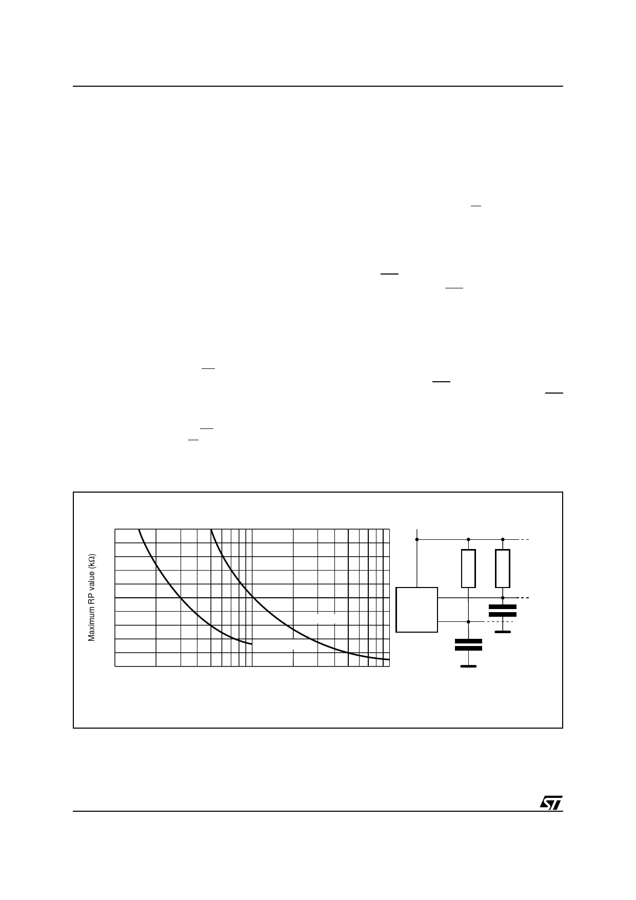
Figure 3. Maximum RL Value versus Bus Capacitance (CBUS) for an I2C Bus
20
16
12
8
4
0
10
VCC
fc = 100kHz
fc = 400kHz
100
CBUS (pF)
RL
SDA
MASTER
SCL
RL
CBUS
1000
CBUS
AI01665
4/16
Share Link: 