EN27LV512200TI 查看數據表(PDF) - Eon Silicon Solution Inc.
零件编号
产品描述 (功能)
生产厂家
EN27LV512200TI Datasheet PDF : 12 Pages
| |||
EN27LV512 / EN27LV512B
EN27LV512 / EN27LV512B 512KBIT EPROM (64K x 8)
FEATURES
• Read Access Time:
-90ns, -120ns, -150ns, -200ns
• Single +3.3V Power Supply
-Regulated power supply 3.0V - 3.6V
(EN27LV512)
-Unregulated power supply 2.7V - 3.6 V
(EN27LV512B for battery operated systems)
• Programming Voltage +12.75V
• QuikRiteTM Programming Algorithm
• Typical programming time 20µs
• Low Power CMOS Operation
• 1µA Standby (Typical)
• 15mA Operation (Max.)
• CMOS- and TTL-Compatible I/O
• High-Reliability CMOS Technology
• Latch-Up Immunity to 100mA
from -1V to VCC + 1V
• Two-Line Control ( OE & CE )
• Standard Product Identification Code
• JEDEC Standard Pinout
• 28-pin PDIP
• 32-pin PLCC
• 28-pin TSOP (Type 1)
• Commercial and Industrial Temperature
Ranges
GENERAL DESCRIPTION
The EN27LV512 / EN27LV512B is a low voltage, low-power 512K bit, 3.3V one-time-
programmable (OTP) read-only memory (EPROM). Organized into 64K words with 8 bits per
word, it features QuikRiteTM single-address location programming, typically at 20µs per byte. Any
byte can be accessed in less than 90ns. The EN27LV512 / EN27LV512B has separate Output
Enable ( OE ) and Chip Enable ( CE ) controls which eliminate bus contention issues. The
EN27LV512 has a Vcc tolerance range of 3.0V to 3.6V, making it suitable for use in systems that
have regulated power supplies. The EN27LV512B has a Vcc tolerance range of 2.7V to 3.6V,
making it ideally suited for battery operated systems.
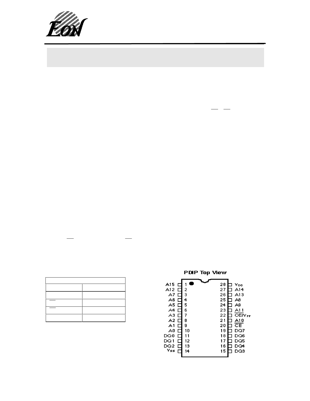
FIGURE 1. PDIP
Pin Name
Function
A0-A15
Addresses
DQ0-DQ7
Outputs
CE
Chip Enable
OE
Output Enable
NC
No Connect
4800 Great America Parkway Ste 202
Santa Clara, CA. 95054
1
Preliminary
Tel: 408-235-8680
Fax: 408-235-8685
Share Link: 