M34C02-RMM1 жҹҘзңӢж•ёж“ҡиЎЁпјҲPDFпјү - STMicroelectronics
йӣ¶д»¶зј–еҸ·
дә§е“ҒжҸҸиҝ° (еҠҹиғҪ)
з”ҹдә§еҺӮ家
M34C02-RMM1 Datasheet PDF : 26 Pages
| |||
M34C02
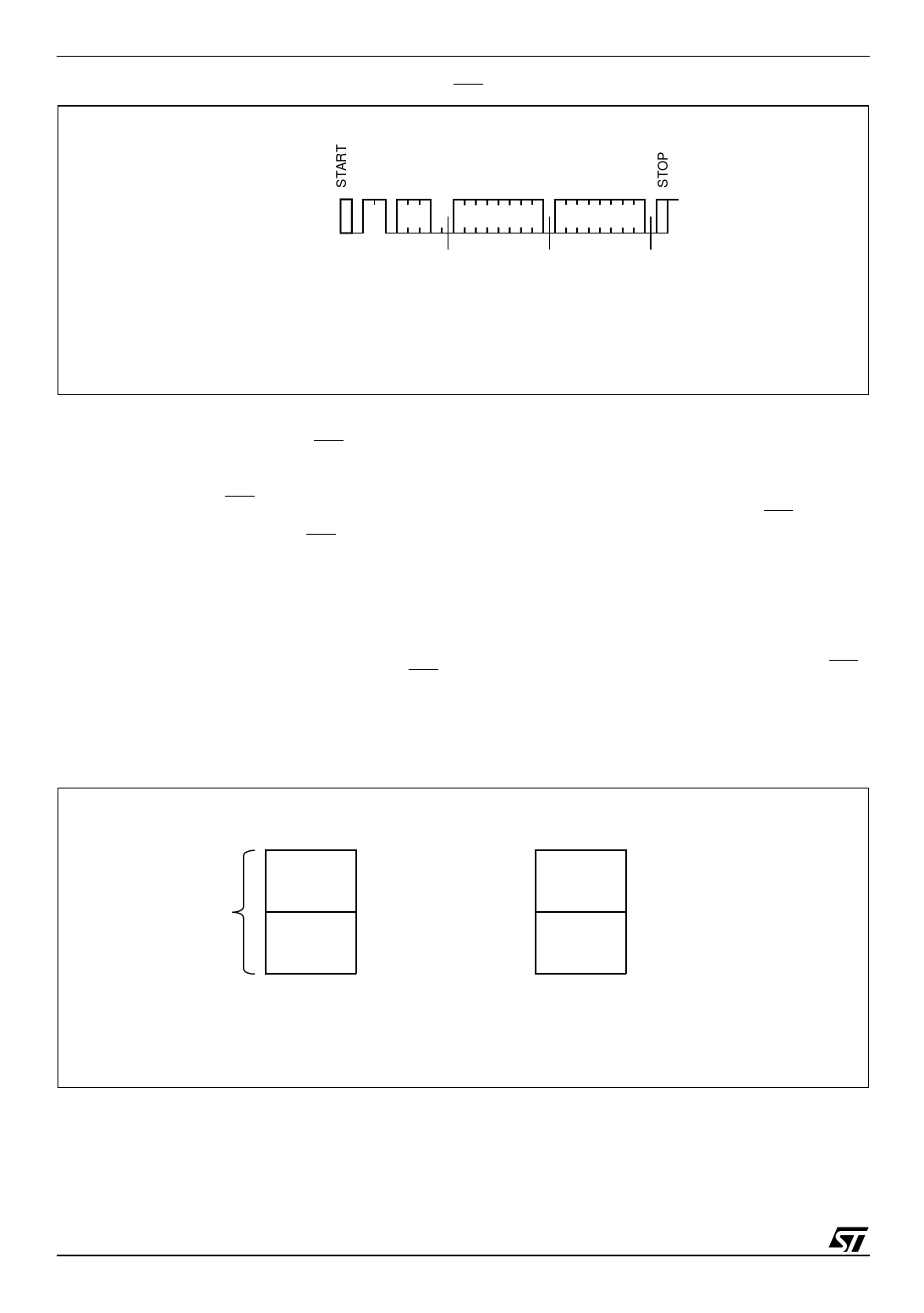
Figure 6. Setting the Write Protection Register (WC = 0)
BUS ACTIVITY
MASTER
SDA LINE
BUS ACTIVITY
CONTROL
BYTE
WORD
ADDRESS
DATA
ACK
ACK
ACK
VALUE
VALUE
(DON'T CARE) (DON'T CARE)
AI01935B
Setting the Software Write-Protection
The M34C02 has a hardware write-protection
feature, using the Write Control (WC) signal. This
signal can be driven High or Low, and must be
held constant for the whole instruction sequence.
When Write Control (WC) is held Low, the whole
memory array (addresses 00h to FFh) is write
protected. When Write Control (WC) is held High,
the write protection of the memory array is
dependent on whether software write-protection
has been set.
Software write-protection allows the bottom half of
the memory area (addresses 00h to 7Fh) to be
permanently write protected irrespective of
subsequent states of the Write Control (WC)
signal.
The write protection feature is activated by writing
once to the Protection Register. The Protection
Register is accessed with the device select code
set to 0110b (as shown in Table 2), and the E2, E1
and E0 bits set according to the states being
applied on the E2, E1 and E0 signals. As for any
other write command, Write Control (WC) needs to
be held Low. Address and data bytes must be sent
with this command, but their values are all ignored,
and are treated as DonвҖҷt Care. Once the
Protection Register has been written, the write
protection of the first 128 bytes of the memory is
enabled, and it is not possible to unprotect these
128 bytes, even if the device is powered off and
on, and regardless the state of Write Control (WC).
When the Protection Register has been written,
the M34C02 no longer responds to the device type
identifier 0110b in either read or write mode.
Figure 7. Result of Setting the Write Protection
Memory
Area
FFh
Standard
Array
80h
7Fh
Standard
Array
00h
Default EEPROM memory area
state before write access
to the Protect Register
FFh
Standard
Array
80h
7Fh
Write
Protected
Array
00h
State of the EEPROM memory
area after write access
to the Protect Register
AI01936C
6/26
Share Link: 