M36W108 查看數據表(PDF) - STMicroelectronics
零件编号
产品描述 (功能)
生产厂家
M36W108
8 Mbit (1Mb x8, Boot Block) Flash Memory and 1 Mbit (128Kb x8) SRAM Low Voltage Multi-Memory Product
STMicroelectronics

M36W108 Datasheet PDF : 35 Pages
| |||
M36W108T, M36W108B
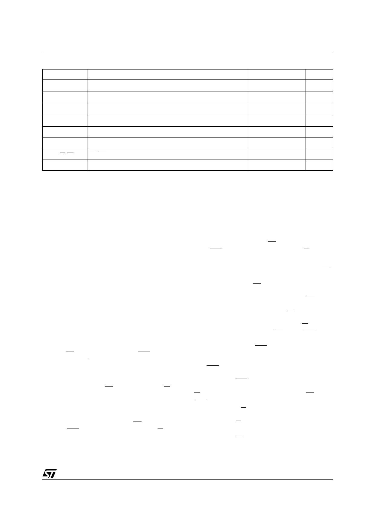
Table 2. Absolute Maximum Ratings (1)
Symbol
Parameter
Value
Unit
TA
Ambient Operating Temperature (3)
–40 to 85
°C
TBIAS
Temperature Under Bias
–50 to 125
°C
TSTG
Storage Temperature
–65 to 150
°C
VIO (2)
Input or Output Voltage
–0.5 to VCC +0.5
V
VCCF
Flash Chip Supply Voltage
–0.6 to 5
V
VCCS
SRAM Chip Supply Voltage
–0.3 to 4.6
V
V(EF, RP)
EF, RP Voltage
0.6 to 13.5
V
PD
Power Dissipation
0.7
W
Note: 1. Except for the rating "Operating Temperature Range", stresses above those listed in the Table "Absolute Maximum Ratings" may
cause permanent damage to the device. These are stress ratings only and operation of the device at these or any other conditions
above those indicated in the Operating sections of this specification is not implied. Exposure to Absolute Maximum Rating condi-
tions for extended periods may affect device reliability. Refer also to the STMicroelectronics SURE Program and other relevant qual-
ity documents.
2. Minimum Voltage may undershoot to –2V during transition and for less than 20ns.
3. Depends on range.
and Chip Erase, Erase Suspend and Resume are
written to the device in cycles of commands to a
Command Interface using standard microproces-
sor write timings.
The SRAM component is a low power SRAM that
features fully static operation requiring no external
clocks or timing strobes, with equal address ac-
cess and cycle times. It requires a single 2.7V to
3.6V VCCS supply, and all inputs and outputs are
TTL compatible.
SIGNAL DESCRIPTIONS
See Figure 1 and Table 1.
Address Inputs (A0-A16). Addresses A0 to A16
are common inputs for the Flash chip and the
SRAM chip. The address inputs for the Flash
memory or the SRAM array are latched during a
write operation on the falling edge of Flash Chip
Enable (EF), SRAM Chip Enable (E1S or E2S) or
Write Enable (W).
Address Inputs (A17-A19). Address A17 to A19
are address inputs for the Flash chip. They are
latched during a write operation on the falling edge
of Flash Chip Enable (EF) or Write Enable (W).
Data Input/Outputs (DQ0-DQ7). The input is
data to be programmed in the Flash or SRAM
memory array or a command to be written to the
C.I. of the Flash chip. Both are latched on the ris-
ing edge of Flash Chip Enable (EF), SRAM Chip
Enable (E1S or E2S) or Write Enable (W). The
output is data from the Flash memory or SRAM ar-
ray, the Electronic Signature Manufacturer or De-
vice codes or the Status register Data Polling bit
DQ7, the Toggle Bits DQ6 and DQ2, the Error bit
DQ5 or the Erase Timer bit DQ3. Outputs are valid
when Flash Chip Enable (EF) or SRAM Chip En-
able (E1S or E2S) and Output Enable (G) are ac-
tive. The output is high impedance when the both
the Flash chip and the SRAM chip are deselected
or the outputs are disabled and when Reset (RP)
is at a VIL.
Flash Chip Enable (EF). The Chip Enable input
for Flash activates the memory control logic, input
buffers, decoders and sense amplifiers. EF at VIH
deselects the memory and reduces the power con-
sumption to the standby level. EF can also be
used to control writing to the command register
and to the Flash memory array, while W remains
at VIL. It is not allowed to set EF at VIL, E1S at VIL
and E2S at VIH at the same time.
SRAM Chip Enable (E1S, E2S). The Chip En-
able inputs for SRAM activate the memory control
logic, input buffers, decoders and sense amplifi-
ers. E1S at VIH or E2S at VIL deselects the mem-
ory and reduces the power consumption to the
standby level. E1S and E2S can also be used to
control writing to the SRAM memory array, while
W remains at VIL. It is not allowed to set EF at VIL,
E1S at VIL and E2S at VIH at the same time.
Output Enable (G). The Output Enable gates the
outputs through the data buffers during a read op-
eration. When G is High the outputs are High im-
pedance.
Write Enable (W). The Write Enable input con-
trols writing to the Command Register of the Flash
chip and Address/Data latches.
3/35
Share Link: