M36W108ABZN 查看數據表(PDF) - STMicroelectronics
零件编号
产品描述 (功能)
生产厂家
M36W108ABZN Datasheet PDF : 36 Pages
| |||

M36W108AT, M36W108AB
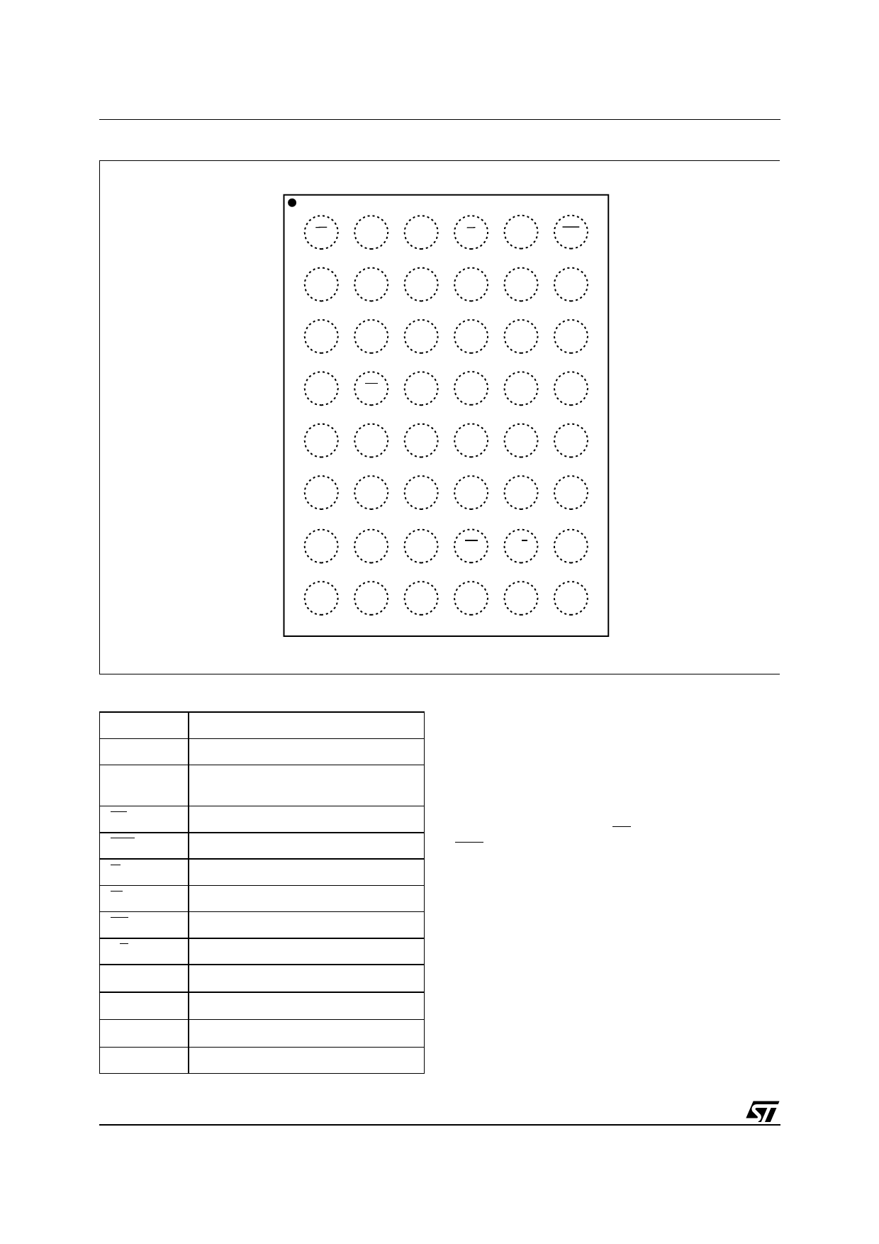
Figure 2. LBGA and LGA Connections (Top View)
1
2
3
4
5
6
A
W
A14
A11
G
A10
E1S
B
VCCS
A18
A8
DQ7
DQ5
VSS
C
A17
NC
A5
DQ4
DQ2
DQ1
D
VSS
EF
NC
DQ0
A0
A1
E
NC
NC
DQ3
A6
A3
A2
F
NC
VCCF
NC
A19
A7
A4
G
NC
DQ6
A13
RP
RB
E2S
H
NC
A12
NC
A16
A15
A9
Table 1. Signal Names
A0-A16
Address Inputs
A17-A19
Address Inputs for Flash Chip
DQ0-DQ7
Data Input/Outputs, Command Inputs
for Flash Chip
EF
Chip Enable for Flash Chip
E1S, E2S
Chip Enable for SRAM Chip
G
Output Enable
W
Write Enable
RP
Reset for Flash Chip
RB
Ready/Busy Output for Flash Chip
VCCF
Supply Voltage for Flash Chip
VCCS
Supply Voltage for SRAM Chip
VSS
Ground
NC
Not Connected Internally
AI02508
DESCRIPTION
The M36W108A is multi-chip device containing an
8 Mbit boot block Flash memory and a 1 Mbit of
SRAM. The device is offered in the new Chip
Scale Package solutions: LBGA48 1.0mm ball
pitch and LGA48 1.0mm land pitch.
The two components, of the package’s overall 9
Mbit of memory, are distinguishable by use of the
three chip enable lines: EF for the Flash memory,
E1S and E2S for the SRAM.
The Flash memory component is identical with the
M29W008A device. It is a non-volatile memory
that may be erased electrically at the block or chip
level and programmed in-system on a Byte-by-
Byte basis using only a single 2.7V to 3.6V VCCF
supply. For Program and Erase operations the
necessary high voltages are generated internally.
The device can also be programmed in standard
programmers. The array matrix organization al-
lows each block to be erased and reprogrammed
without affecting other blocks.
Instructions for Read/Reset, Auto Select for read-
ing the Electronic Signature, Programming, Block
2/36