M470L3224BT0 查看數據表(PDF) - Samsung
零件编号
产品描述 (功能)
生产厂家
M470L3224BT0 Datasheet PDF : 14 Pages
| |||
M470L3224BT0
200pin DDR SDRAM SODIMM
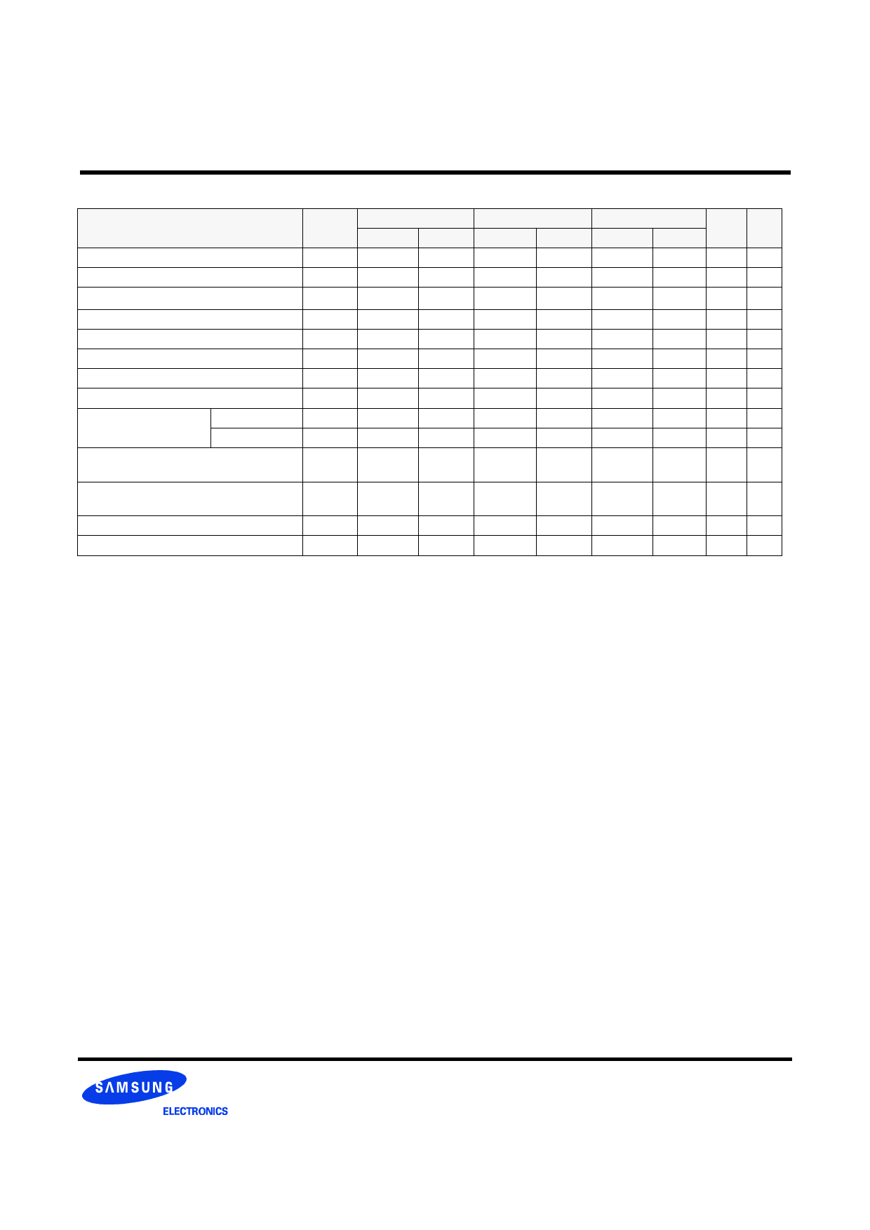
Parameter
Mode register set cycle time
DQ & DM setup time to DQS
DQ & DM hold time to DQS
DQ & DM input pulse width
Power down exit time
Exit self refresh to write command
Exit self refresh to bank active command
Exit self refresh to read command
Refresh interval time
64Mb, 128Mb
256Mb
Output DQS valid window
Clock half period
Data hold skew factor
DQS write postamble time
-TCA2(DDR266A)
Symbol
Min
Max
-TCB0(DDR266B)
Min
Max
-TCA0 (DDR200)
Min
Max
tMRD
15
15
16
tDS
0.5
0.5
0.6
tDH
0.5
0.5
0.6
tDIPW 1.75
1.75
2
tPDEX
10
10
10
tXSW
95
116
tXSA
75
75
80
tXSR
200
200
200
tREF
15.6
15.6
15.6
7.8
7.8
7.8
tQH
tHPmin
-tQHS
-
tHPmin
-tQHS
-
tHPmin
-tQHS
-
tHP
tCLmin
or tCHmin
-
tCLmin
or tCHmin
-
tCLmin
or tCHmin
-
tQHS
0.75
0.75
0.8
tWPST 0.25
0.25
0.25
Unit Note
ns
ns 7,8,9
ns 7,8,9
ns
ns
ns
ns 4
Cycle
us 1
us 1
ns 5
ns
ns
tCK 3
Note : 1. Maximum burst refresh of 8
2. The specific requirement is that DQS be valid(High or Low) on or before this CK edge. The case shown(DQS going from
High_Z to logic Low) applies when no writes were previously in progress on the bus. If a previous write was in progress,
DQS could be High at this time, depending on tDQSS.
3. The maximum limit for this parameter is not a device limit. The device will operate with a great value for this parameter,
but system performance (bus turnaround) will degrade accordingly.
4. A write command can be applied with tRCD satisfied after this command.
5. For registered DINNs, tCL and tCH are ≥ 45% of the period including both the half period jitter (tJIT(HP)) of the PLL and the half
period jitter due to crosstalk (tJIT(crosstalk)) on the DIMM.
Rev. 0.1 June. 2001
Share Link: 