M48T59VMH жҹҘзңӢж•ёж“ҡиЎЁпјҲPDFпјү - STMicroelectronics
йӣ¶д»¶зј–еҸ·
дә§е“ҒжҸҸиҝ° (еҠҹиғҪ)
з”ҹдә§еҺӮ家
M48T59VMH Datasheet PDF : 21 Pages
| |||
M48T59, M48T59Y, M48T59V
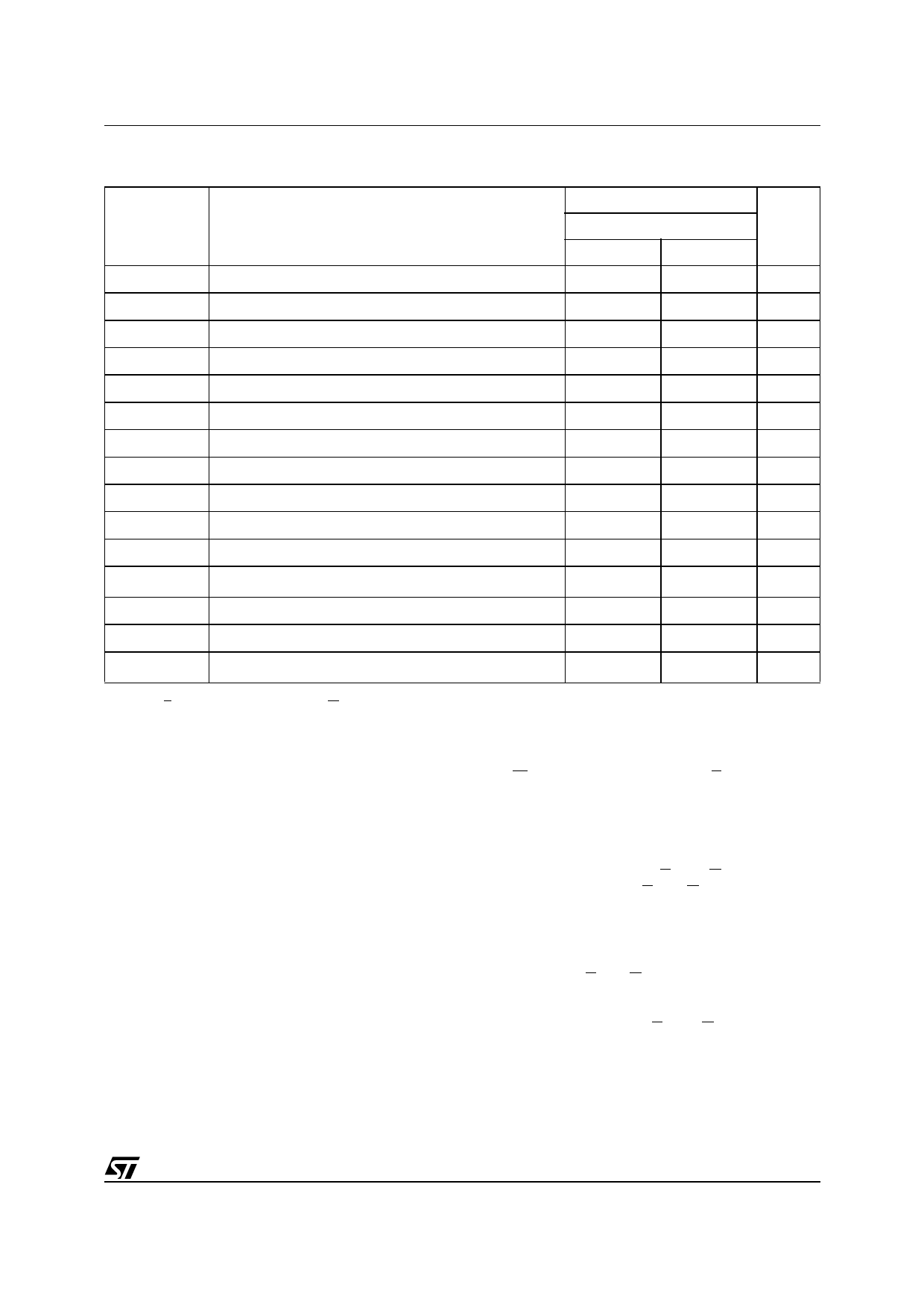
Table 10. Write Mode AC Characteristics
(TA = 0 to 70 В°C or вҖ“40 to 85 В°C; VCC = 4.75V to 5.5V or 4.5V to 5.5V or 3.0V to 3.6V)
M48T59/M48T59Y/M48T59V
Symbol
Parameter
-70
Min
Max
tAVAV
Write Cycle Time
70
tAVWL
Address Valid to Write Enable Low
0
tAVEL
Address Valid to Chip Enable Low
0
tWLWH
Write Enable Pulse Width
50
tELEH
Chip Enable Low to Chip Enable High
55
tWHAX
Write Enable High to Address Transition
0
tEHAX
Chip Enable High to Address Transition
0
tDVWH
Input Valid to Write Enable High
30
tDVEH
Input Valid to Chip Enable High
30
tWHDX
Write Enable High to Input Transition
5
tEHDX
Chip Enable High to Input Transition
5
tWLQZ (1, 2) Write Enable Low to Output Hi-Z
25
tAVWH
Address Valid to Write Enable High
60
tAVE1H
Address Valid to Chip Enable High
60
tWHQX (1, 2) Write Enable High to Output Transition
5
Note: 1. CL = 5pF (see Fig 4).
2. If E goes low simultaneously with W going low, the outputs remain in the high impedance state.
Unit
ns
ns
ns
ns
ns
ns
ns
ns
ns
ns
ns
ns
ns
ns
ns
The eight clock bytes are not the actual clock
counters themselves; they are memory locations
consisting of BiPORTв„ў read/write memory cells.
The M48T59/59Y/59V includes a clock control cir-
cuit which updates the clock bytes with current in-
formation once per second. The information can
be accessed by the user in the same manner as
any other location in the static memory array.
The M48T59/59Y/59V also has its own Power-fail
Detect circuit. The control circuitry constantly mon-
itors the single 5V supply for an out of tolerance
condition. When VCC is out of tolerance, the circuit
write protects the SRAM, providing a high degree
of data security in the midst of unpredictable sys-
tem operation brought on by low VCC. As VCC falls
below approximately 3V, the control circuitry con-
nects the battery which maintains data and clock
operation until valid power returns.
READ MODE
The M48T59/59Y/59V is in the Read Mode when-
ever W (Write Enable) is high and E (Chip Enable)
is low. The unique address specified by the 13 Ad-
dress Inputs defines which one of the 8,192 bytes
of data is to be accessed. Valid data will be avail-
able at the Data I/O pins within Address Access
time (tAVQV) after the last address input signal is
stable, providing that the E and G access times
are also satisfied. If the E and G access times are
not met, valid data will be available after the latter
of the Chip Enable Access time (tELQV) or Output
Enable Access time (tGLQV).
The state of the eight three-state Data I/O signals
is controlled by E and G. If the outputs are activat-
ed before tAVQV, the data lines will be driven to an
indeterminate state until tAVQV. If the Address In-
puts are changed while E and G remain active,
output data will remain valid for Output Data Hold
time (tAXQX) but will go indeterminate until the next
Address Access.
7/21
Share Link: 