M5482B7(1993) 查看數據表(PDF) - STMicroelectronics
零件编号
产品描述 (功能)
生产厂家
M5482B7 Datasheet PDF : 6 Pages
| |||
M5482
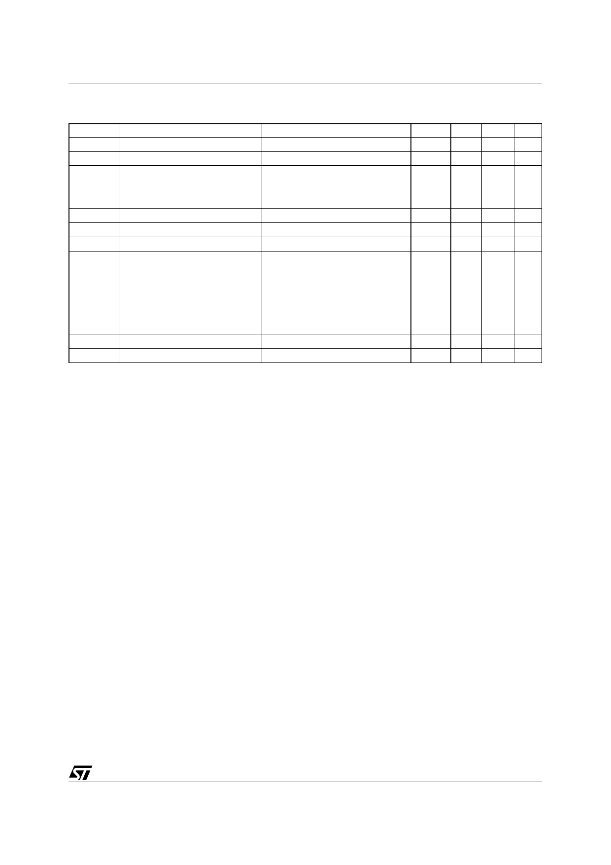
STATIC ELECTRICAL CHARACTERISTICS
(Tamb within operating range, VDD = 4.75V to 13.2V, VSS = 0V,unless otherwise specified)
Symbol
Parameter
Test Conditions
Min. Typ. Max.
VDD Supply Voltage
IDD Supply Current
VI
Input Voltages
Logical "0" Level
Logical "1" Level
IB
Brightness Input Current (note 2)
VB Brightness Input Voltage (pin 9)
VO(off)
IO
Off State Output Voltage
Output Sink Current (note 3)
Segment OFF
Segment ON
VDD = 13.2 V
± 10 µA Input Bias
4.75 ≤ VDD ≤ 5.25
VDD > 5.25
Input Current
Tamb = 25oC
=
750
µA
VO = 3 V
VO = 1 V (note 4)
Brightness In. = 0 µA
Brightness In. = 100 µA
Brightness In. = 750 µA
4.75
– 0.3
2.2
VDD – 2
0
3
0
2
2.7
12
15
13.2
7
0.8
VDD
VDD
0.75
4.3
13.2
10
10
4
25
fclock Input Clock Frequency
IO
Output Matching (note 1)
0
0.5
± 20
Notes : 1. Output matching is calculated as the percent variation from IMAX + IMIN/2.
2. With a fixed resistor on the brightness input some variation in brightness will occur from one device to another.
3. Absolute maximum for each output should be limited to 40 mA.
4. The VO voltage should be regulated by the user.
Unit
V
mA
V
V
V
mA
V
V
µA
µA
mA
mA
MHz
%
FUNCTIONAL DESCRIPTION
The M5482 uses the M5451 die which is packaged
to operate 2-digit alphanumeric displays with mini-
mal interface with the display and the data source.
Serial data transfer from the data source to the
display driver is accomplished with 2 signals, serial
data and clock. Using a format of a leading "1"
followed by the 35 data bits allows data transfer
without an additional load signal.
The 35 data bits are latched after the 36th bit is
complete, thus providing non-multiplexed, direct
drive to the display. Outputs change only if the
serial data bits differ from the previous time. Display
brightness is determined by control of the output
Figure 2 : Input Data Format
1
CLOCK
DATA
START BIT 1
current for LED displays. A 1nF capacitor should be
connected to brightness control, Pin 9, to prevent
possible oscillations.
A block diagram is shown in Figure 1. The output
current is typically 20 times greater than the current
into Pin 9, which is set by an external variable
resistor.
There is an internal limiting resistor of 400Ω nomi-
nal value.
Figure 2 shows the input data format. A start bit of
logical "1" precedes the 35 bits of data. At the 36th
clock a LOAD signal is generated synchronously
with the high state of the clock, which loads the 35
bits of the shift registers into the latches.
36
BIT 34 BIT 35
LOAD
(INTERNAL)
RESET
(INTERNAL)
3/6
Share Link: 