M58BF008ZA 查看數據表(PDF) - STMicroelectronics
零件编号
产品描述 (功能)
生产厂家
M58BF008ZA Datasheet PDF : 36 Pages
| |||
M58BF008
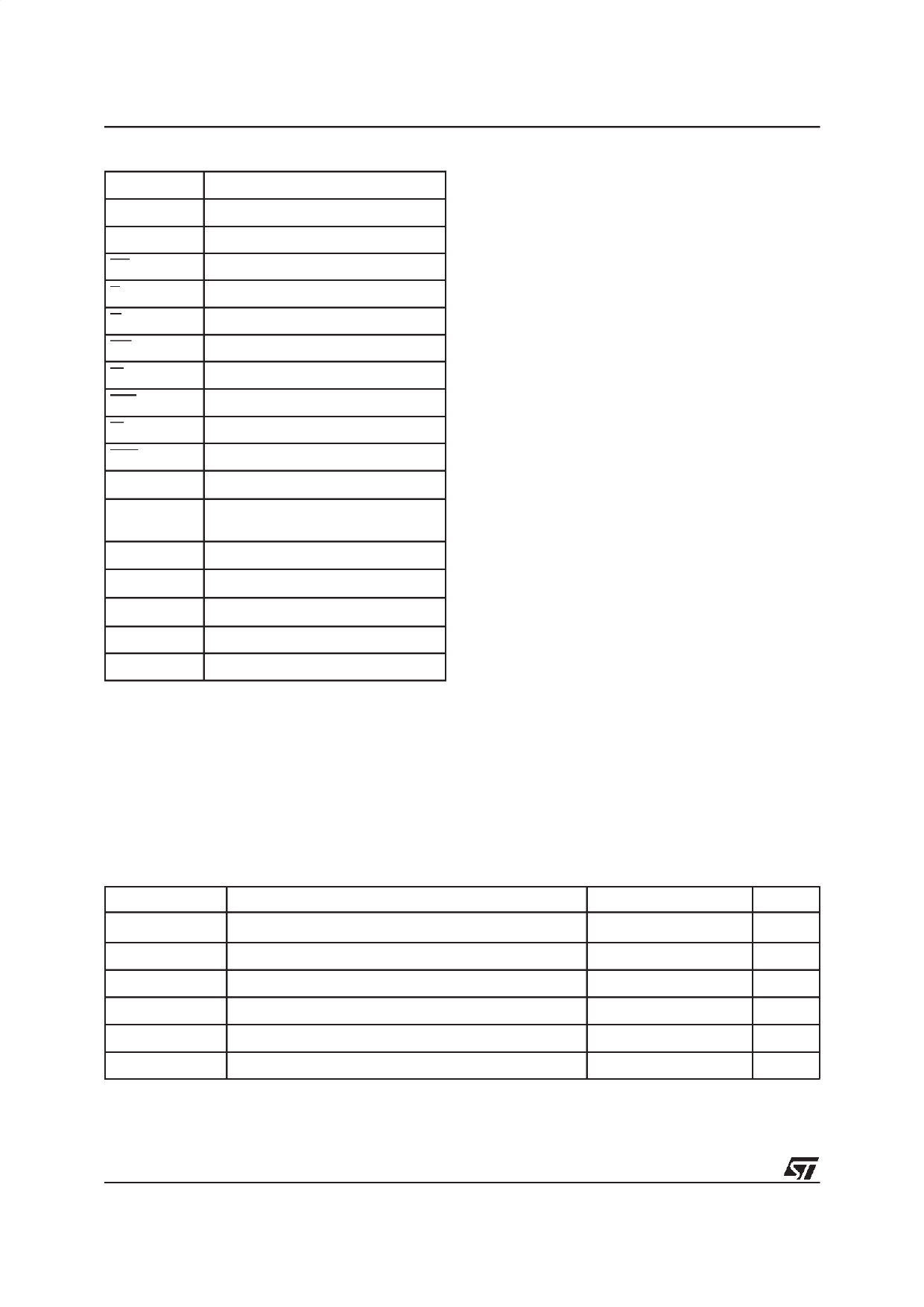
Table 1. Signal Names
A0-A17
Address Inputs
DQ0-DQ31 Data Input/Output
CLK
System Clock
RP
Reset/Power-down
E
Chip Enable
G
Output Enable
GD
Output Disable
W
Write Enable
LBA
Load Burst Address
WR
Write/Read
BAA
Burst Address Advance
VDD
Supply Voltage
VDDQ
Supply Voltage for Input/Output
Buffers
VPP
Program Supply Voltage
VSS
Ground
VSSQ
Input/Output Ground
NC
Not Connected Internally
DU
Don’t Use as Internally Connected
A Command Interface decodes the Instructions
written to the memory to access or modify the
memory content, to toggle the enable/disable of
read access to the Overlay block, to toggle the
burst Wrap/No-wrap or to toggle the Synchronous
or Asynchronous Read mode. A Program/Erase
Controller (P/E.C.) executes the algorithms taking
care of the timings necessary for program and
erase operations. The P/E.C. also takes care of
verification to unburden the system microproces-
sor, while a Status Register tracks the status of
each operation.
The following Instructions are executed by the
memory in either Asynchronous or Synchronous
mode.
Access or modify memory content:
- Read Array
- Read or Clear Status Register
- Read Electronic Signature
- Erase Main memory block or Overlay block
- Program Main memory or Overlay memory
- Program Erase Suspend or Resume
Toggle:
– Asynchronous/Synchronous Read
– Overlay Block Read Enable/Disable
– Burst Wrap/No-wrap
The M58BF008 devices are offered in PQFP80
and LBGA80 1.0mm ball pitch packages.
When the VPP supply is at VSS this prevents pro-
gramming and erasure of the memory blocks and,
in addition, it prevents reading of the Overlay
block. When the VPP supply is at 5V it enables
both in-system program/erase and read access to
the Overlay block. For a limited time and number
of program/erase cycles the VPP supply may be
raised to 12V to provide fast program and erase
times.
Table 2. Absolute Maximum Ratings (1)
Symbol
Parameter
Value
Unit
TA
Ambient Operating Temperature
–40 to 125
°C
TBIAS
Temperature Under Bias
–40 to 125
°C
TSTG
Storage Temperature
–55 to 150
°C
VIO
Input Output Voltage
–0.6 to VDDQ +0.6
V
VDD, VDDQ
Supply Voltage
–0.6 to 7
V
VPP
Program Voltage
–0.6 to 13.5
V
Note: 1. Stresses above those listed in the Table ”Absolute Maximum Ratings” may cause permanent damage to the device.
4/36
Share Link: 