M58BF008ZA 查看數據表(PDF) - STMicroelectronics
零件编号
产品描述 (功能)
生产厂家
M58BF008ZA Datasheet PDF : 36 Pages
| |||
M58BF008
DEVICE OPERATIONS
See Table 4 for Asynchronous or Synchronous
Bus Operations.
In the Asynchronous mode the memory is selected
with Chip Enable E Low. The data outputs are en-
abled by Output Enable G Low or disabled by Out-
put Disable GD Low. Data is input by Write Enable
W Low.
In the Synchronous mode the memory latches ad-
dresses and data (input or output) on the rising
edge of the System Clock CLK. Burst address
latching is enabled by Load Burst Address LBA
Low with Write/Read WR Low for a write cycle or
High for a read cycle.
Data outputs are enabled for reading on the rising
edge of the System Clock CLK when Output En-
able G is low. Data is input on the rising edge of
the System Clock CLK when Write Enable W is
Low.
The memory is deselected and in standby mode
when Chip Enable E is High, and it is reset or in
power-down mode when Reset/Power-Down RP
is Low.
Read. Read operations are used to output the
contents of the memory, the Electronic Signature
or the Status Register. The data read depends on
the previous Instruction given to the memory.
Read operations can be Asynchronous or Syn-
chronous, with a single or burst read. On power-up
the device is in Asynchronous read mode, the In-
struction Asynchronous/Synchronous Read Tog-
gle ART can be used to enter the Synchronous
read mode.
– Asynchronous Read. To read a data Double-
Word in Asynchronous mode the address inputs
must be stable and Chip Enable E must be Low
during the read cycle. Output Enable G must be
Low and Output Disable GD High. The Load
Burst Address LBA is Don’t Care, but its falling
edge will start a new read cycle.
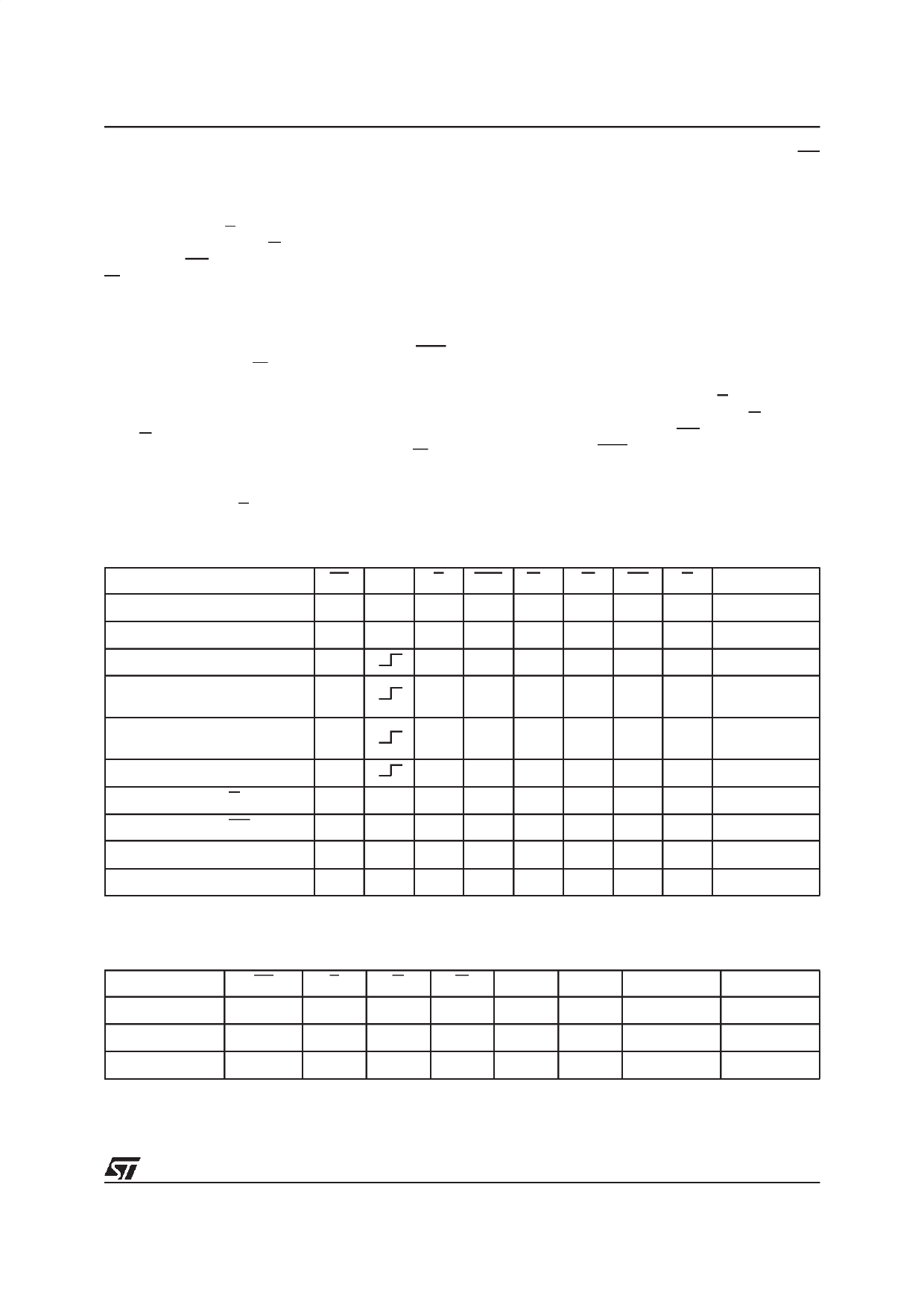
Table 4. Bus Operations (1,2)
Op eration
RP CLK E LBA WR
W
GD
G
DQ0-DQ31
Asynchronous Read
VIH
X
VIL
X
X
VIH
VIH
VIL
Data Output
Asynchronous Write
VIH
X
VIL
X
X
VIL
VIH
VIH
Data Input
Synchronous Read
VIH
VIL
VIH
VIH
X
VIH
VIL
Data Output
Synchronous Write Address for
Read
VIH
VIL
VIL
VIH
X
VIH
VIH
X
Synchronous Write Address for
Command
VIH
VIL
VIL
VIL
X
VIH
VIH
X
Synchronous Data Write
VIH
VIL
VIH
VIH
VIL
VIH
VIH
Data Input
Output Disabled by G
VIH
X
VIL
X
X
X
VIH
VIH
Hi-Z
Output Disabled by GD
VIH
X
VIL
X
X
X
VIL
X
Hi-Z
Standby
VIH
X
VIH
X
X
X
X
X
Hi-Z
Reset / Power-down
VIL
X
X
X
X
X
X
X
Hi-Z
Note: 1. See Device Operations, Instructions and Commands, sections for more details.
2. X=VIL or VIH.
Table 5. Read Electronic Signature
Code
RP
E
G
W
A0
Manufacturer
VIH
VIL
VIL
VIH
VIL
Device
VIH
VIL
VIL
VIH
VIH
Version
VIH
VIL
VIL
VIH
VIL
Note: ”x” = version level. The first version is ”0” and it can have a value up to ”7”.
A1
A2-A17
DQ0-DQ31
VIL
Don’t Care 00000020h
VIL
Don’t Care 000000F0h
VIH
Don’t Care 0000000xh
7/36
Share Link: 