M5M54R16AJ 查看數據表(PDF) - MITSUBISHI ELECTRIC
零件编号
产品描述 (功能)
生产厂家
M5M54R16AJ Datasheet PDF : 7 Pages
| |||
MITSUBISHI LSIs
M5M54R16AJ,ATP-10,-12,-15
4194304-BIT (262144-WORD BY 16-BIT) CMOS STATIC RAM
ABSOLUTE MAXIMUM RATINGS
Symbol
V cc
VI
VO
Pd
T opr
Parameter
Supply voltage
Input voltage
Output voltage
Power dissipation
Operating temperature
Conditions
With respect to GND
Ta=25°C
Ratings
Unit
- 2.0*~ 4.6
V
- 2.0*~ Vcc+0.5 V
- 2.0*~ Vcc
V
1000
mW
0 ~ 70
°C
Tstg(bias) Storage temperature(bias)
- 10 ~ 85
°C
Tstg
Storage temperature
- 65 ~ 150
°C
*Pulse width ≤3ns, In case of DC: - 0.5V
+10%
DC ELECTRICAL CHARACTERISTICS (Ta=0~70°C, Vcc=3.3V -5% ,unless otherwise noted)
Symbol
Parameter
Condition
Limits
Unit
Min Typ Max
VIH High-level input voltage
VIL Low-level input voltage
VOH High-level output voltage IOH = - 4mA
2.0
Vcc+0.3 V
0.8 V
2.4
V
VOL Low-level output voltage IOL= 8mA
II
Input current
V I = 0 ~ Vcc
IOZ
Output current in off-state
VI (S)= VIH
VO= 0 ~ Vcc
0.4 V
2 uA
2 uA
Active supply current
I CC1 (TTL level)
VI (S)= VIL
other inputs VIH or VIL
Output-open(duty 100%)
AC(10ns cycle)
AC(12ns cycle)
AC(15ns cycle)
DC
260
250
230
mA
120
AC(10ns cycle)
90
I CC2
Stand-by supply current
(TTL level)
VI (S)= VIH
AC(12ns cycle)
AC(15ns cycle)
70
60 mA
DC
Stand-by current
I CC3 (MOS level)
VI (S)= Vcc - 0.2V
other inputs VI≤0.2V
or VI≥Vcc - 0.2V
40
10 mA
Note 1: Direction for current flowing into an IC is positive (no mark).
CAPACITANCE
(Ta=0~70°C
+10%
, Vcc=3.3V -5% ,unless otherwise noted)
Symbol
Parameter
Test Condition
C I Input capacitance
CO Output capacitance
VI =GND,Vi =25mVrms,f=1MHz
Vo =GND,Vo =25mVrms,f=1MHz
Note 2: CI,CO are periodically sampled and are not 100% tested.
Min
Limit
Typ Max
Unit
7 pF
8 pF
AC
ELECTRICAL
CHARACTERISTICS
(Ta=
0~70
°C
,VCC=3.3V
+10%
-5%
,unless
otherwise
noted)
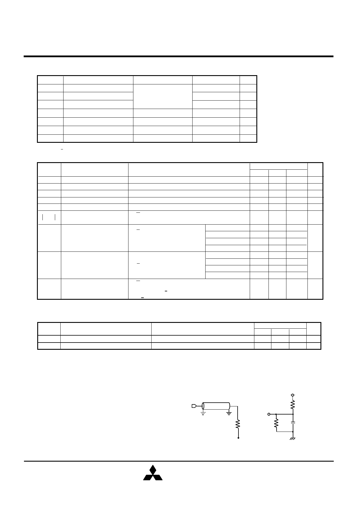
(1) MEASUREMENT CONDITION
Input pulse levels ................................... VIH=3.0V,VIL=0.0V
Input rise and fall time ................................................... 3ns
Input timing reference levels ...................... VIH=1.5V,VIL=1.5V
Output timing reference levels ................ VOH=1.5V, VOL=1.5V
Output loads ....................................................... Fig1 ,Fig2
OUTPUT
Z0=50Ω
RL=50Ω
VL=1.5V
DQ DQ
5.0V
480Ω
255Ω 5pF
( ) Including
scope and JIG
Fig.1 Output load
Fig.2 Output load for t en, t dis
MITSUBISHI
ELECTRIC
3
Share Link: 