M5M5W816WG-85L 查看數據表(PDF) - MITSUBISHI ELECTRIC
零件编号
产品描述 (功能)
生产厂家
M5M5W816WG-85L Datasheet PDF : 8 Pages
| |||
1999.1.15 Ver. 0.1
MITSUBISHI LSIs
M5M5W816WG -85L, 10L, 85H, 10H
-85LI, 10LI, 85HI, 10HI
PRELIMINARY
Notice: This is not a final specification.
Some parametric limits are subject to change
8388608-BIT (524288-WORD BY 16-BIT) CMOS STATIC RAM
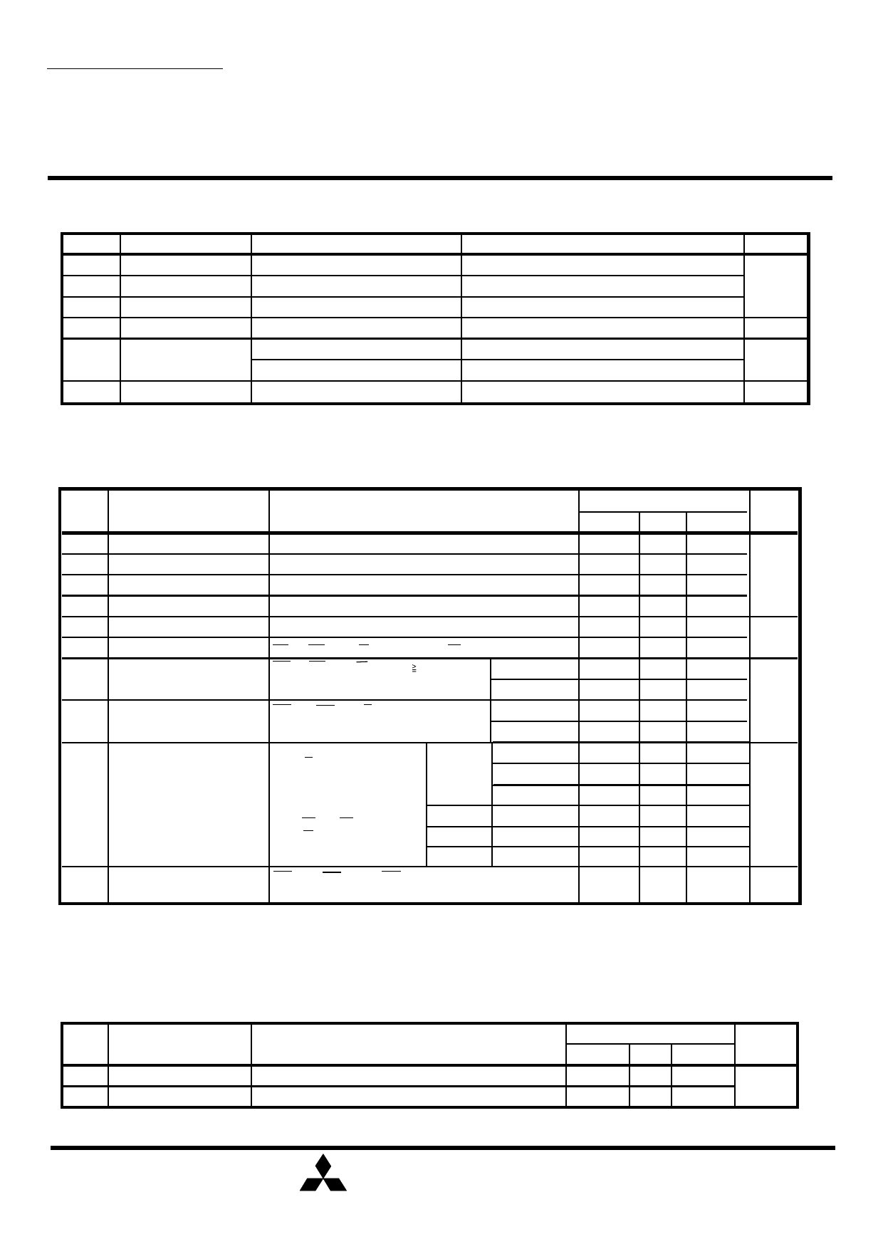
ABSOLUTE MAXIMUM RATINGS
Symbol
Parameter
Vcc Supply voltage
VI
Input voltage
VO Output voltage
Pd
Power dissipation
Operating
Ta
temperature
Tstg Storage temperature
Conditions
With respect to GND
With respect to GND
With respect to GND
Ta=25∞C
Standard (-L, -H)
I-version (-LI, -HI)
Ratings
-0.5* ~ +4.6
-0.2* ~ Vcc + 0.2 (max. 4.6V)
0 ~ Vcc
700
0 ~ +70
- 40 ~ +85
- 65 ~ +150
* -3.0V in case of AC (Pulse width <= 30ns)
Units
V
mW
°C
°C
DC ELECTRICAL CHARACTERISTICS
( Vcc=1.8 ~ 2.7V, unless otherwise noted)
Symbol
Parameter
VIH High-level input voltage
VIL Low-level input voltage
VOH High-level output voltage
VOL Low-level output voltage
II Input leakage current
IO Output leakage current
Icc1 Active supply current
( AC,MOS level )
Active supply current
Icc2
( AC,TTL level )
Icc3 Stand by supply current
( AC,MOS level )
Stand by supply current
Icc4
( AC,TTL level )
Conditions
IOH= -0.1mA
IOL=0.1mA
VI =0 ~ Vcc
BC1 and BC2=VIHor S1=VIHor S2=VIL or OE=VIH, VI/O=0 ~ Vcc
BC1 and BC2<= 0.2V, S1<= 0.2V, S2 Vcc-0.2V
other inputs <=0.2V or => Vcc-0.2V
Output - open (duty 100%)
f= 10MHz
f= 1MHz
BC1 and BC2=VIL , S=VIL ,S2=VIH
other pins =VIH or VIL
Output - open (duty 100%)
f= 10MHz
f= 1MHz
(1) S1 => Vcc - 0.2V,
other inputs = 0 ~ Vcc
(2) S2=> 0.2V,
other inputs = 0 ~ Vcc
(3) BC1 and BC2 =>Vcc - 0.2V
S1 <=0.2V, S2 =>Vcc - 0.2V
other inputs = 0 ~ Vcc
-H, -HI
-HI
-L, -LI
-LI
~ +25°C
~ +40°C
~ +70°C
~ +85°C
~ +70°C
~ +85°C
BC1 and BC2=VIH or S1=VIH or S2=VIL
Other inputs= 0 ~ Vcc
Limits
Min Typ
Max Units
0.7 x Vcc
Vcc+0.2V
-0.2 *
1.6
0.4
V
0.2
±1
µA
±1
-
40 50
-
5
10
-
40 50
mA
-
5
10
-
0.1 1
-
0.2 2
-
-
8
-
-
15
µA
-
-
16
-
-
30
-
-
0.5 mA
Note 1: Direction for current flowing into IC is indicated as positive (no mark)
* -1.0V in case of AC (Pulse width =< 30ns)
Note 2: Typical parameter indicates the value for the center of distribution at 2.7V, and not 100% tested.
CAPACITANCE
Symbol Parameter
CI
Input capacitance
CO Output capacitance
Conditions
VI=GND, VI=25mVrms, f=1MHz
VO=GND,VO=25mVrms, f=1MHz
(Vcc=1.8 ~ 2.7V, unless otherwise noted)
Limits
Min Typ Max
10
10
Units
pF
MITSUBISHI ELECTRIC
3
Share Link: 